Printed circuit board unit and electronic apparatus

a technology of printed circuit boards and electronic devices, applied in the direction of electrical apparatus contruction details, association of printed circuit non-printed electric components, coupling device connections, etc., can solve the problems of insufficient noise removal of transformers and easy to reach noise, and achieve the effect of suppressing nois

Inactive Publication Date: 2007-12-04
FUJITSU LTD
View PDF6 Cites 4 Cited by
  • Summary
  • Abstract
  • Description
  • Claims
  • Application Information

AI Technical Summary

Benefits of technology

[0008]The printed circuit board unit enables disposition of the power source layer in the printed circuit board at a position outside the peripheral section. The noise cut filter is located on the surface of the printed circuit board at the second section inside the peripheral section, so that the noise cut filter is allowed to operate without receiving any influence of noise from the power source layer. Noise is sufficiently removed at the noise cut filter. Noise is suppressed to the utmost in electric signals in the connector. Radiation of noise is reliably reduced at the connector. Electromagnetic interference can be suppressed.
[0009]The power source layer may be located off the first and second sections. The connector is located at the first section. Accordingly, the connector is allowed to operate without receiving any influence of noise from the power source layer. Noise is sufficiently removed at the connector in the same manner as mentioned above. Radiation of noise is reliably reduced at the connector. Electromagnetic interference can be suppressed.
[0010]The printed circuit board unit may further comprise an electrically conductive ground layer crossing between the second and third sections within the peripheral section. The ground layer is thus allowed to serve as a shield. The electrically conductive ground layer may be formed within the printed circuit board at least off the first and second sections. The noise cut filter and the connector are thus allowed to operate without receiving any influence of noise from the power source layer. Noise is sufficiently removed at the noise cut filter. Noise is suppressed to the utmost in electric signals in the connector. Radiation of noise is reliably reduced at the connector. Electromagnetic interference can be suppressed.
[0011]The printed circuit board unit may further comprise a coupling member contacting with the ground layer. In this case, the coupling member may protrude from the printed circuit board. The coupling member may be screwed into a frame member, for example. If the frame member is made of an metallic material, electric current is allowed to flow in the frame member through the coupling member from the ground layer. The characteristic impedance of the ground layer can sufficiently be reduced.

Problems solved by technology

If the transformer is exposed within a larger noise transferred from the power source and ground layers, the transformer cannot sufficiently remove the noise.
The noise tends to reach the connector through the signal line pattern.

Method used


Image

  • Printed circuit board unit and electronic apparatus
  • Printed circuit board unit and electronic apparatus
  • Printed circuit board unit and electronic apparatus

Examples


Embodiment Construction

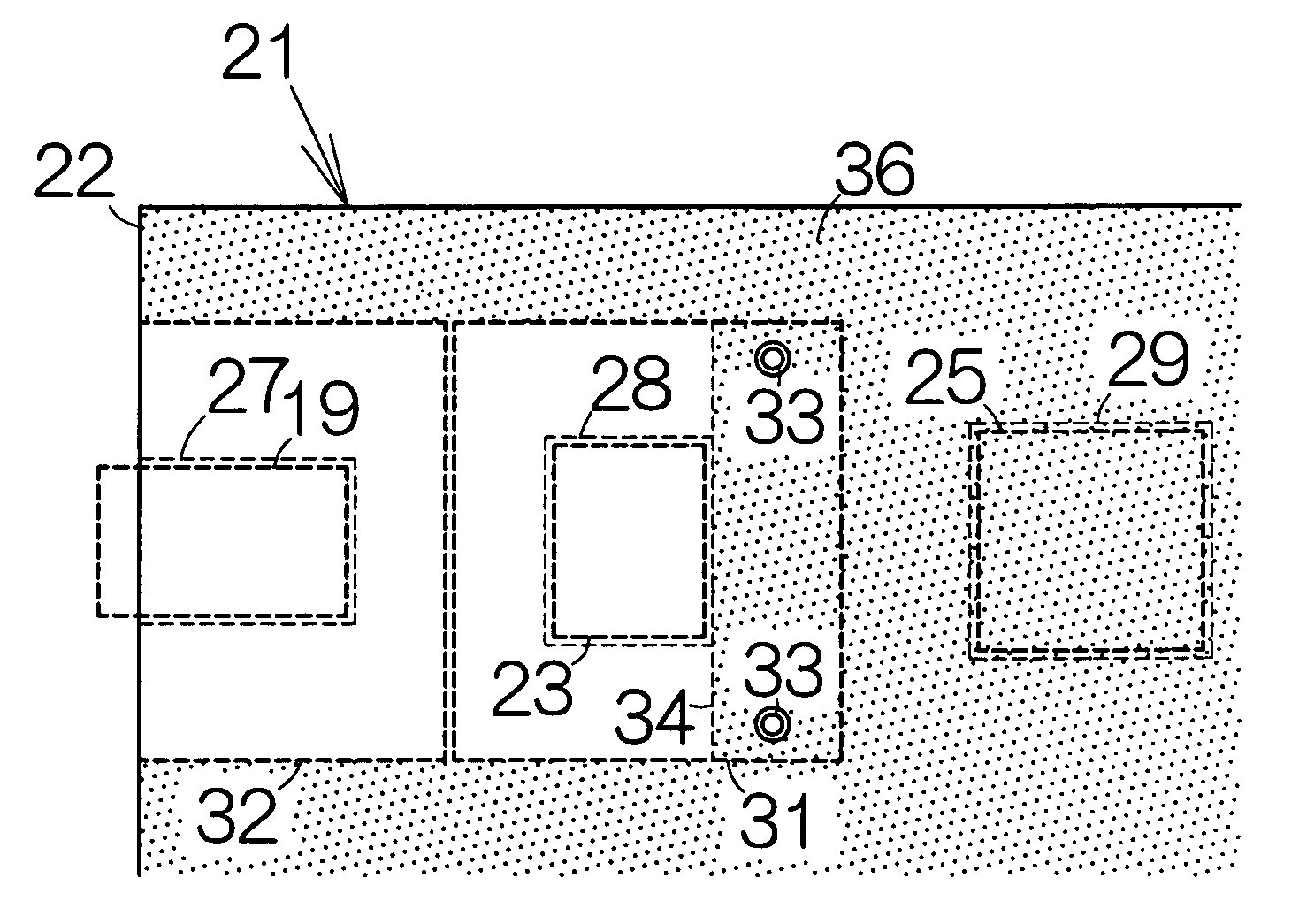
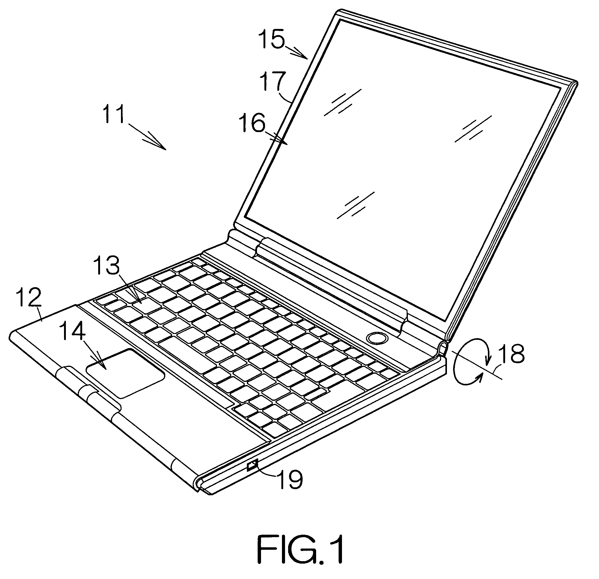
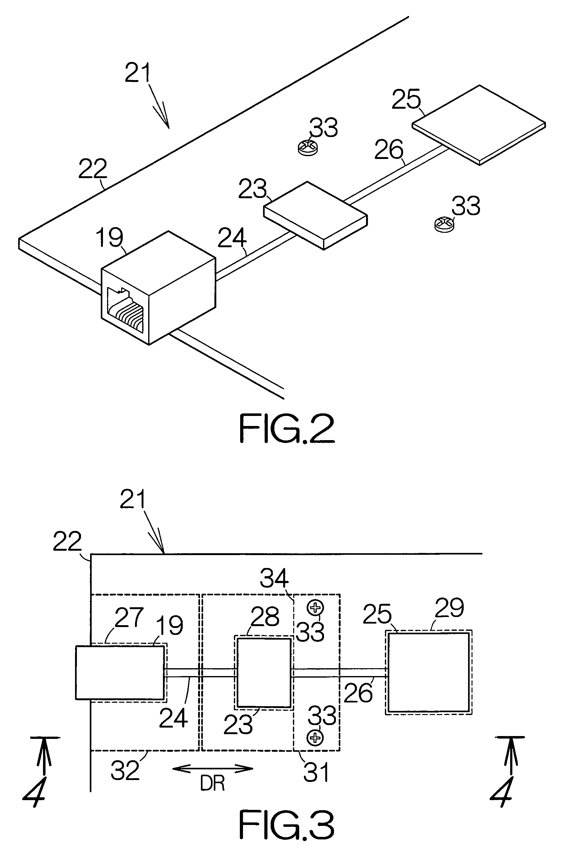
[0024]FIG. 1 schematically illustrates a notebook personal computer 11 as an example of an electronic apparatus according to an embodiment of the present invention. The notebook personal computer 11 includes a main enclosure 12 containing a motherboard, for example. Electronic circuit components such as a central processing unit (CPU) and a memory are mounted on the motherboard. The CPU implements various processings based on software programs and data temporarily stored in the memory, for example. The software programs and data may be stored in a mass storage device such as a hard disk drive (HDD) likewise contained within the main enclosure 12.

[0025]Input devices such as a keyboard 13 and a pointing device 14 are incorporated in the main enclosure 12. The user of the notebook personal computer 11 is allowed to input various instructions and data to the CPU through the input devices 13, 14. A touch pad may be employed as the pointing device 14, for example.

[0026]A display device 15...


PUM


Abstract

A printed circuit board has separate first, second and third sections arranged in a predetermined direction. A connector is mounted at the first section. A noise cut filter is mounted at the second section and connected to the connector. An electronic circuit component is mounted at the third section and connected to the noise cut filter. An electrically conductive power source layer is formed within the printed circuit board at a position outside a peripheral section adjacent the second section. The noise cut filter is allowed to operate without receiving any influence of noise from the power source layer. Noise is sufficiently removed at the noise cut filter. Noise is suppressed to the utmost in electric signals in the connector. Radiation of noise is reliably reduced at the connector. Electromagnetic interference can be suppressed.

Description

BACKGROUND OF THE INVENTION[0001]1. Field of the Invention[0002]The present invention relates to an electronic apparatus. In particular, the invention relates to a printed circuit board unit including a printed circuit board and an electronic circuit component mounted on the surface of the printed circuit board.[0003]2. Description of the Prior Art[0004]For example, a printed circuit board unit often includes a power source layer and a ground layer formed within a printed circuit board, as disclosed in Japanese Patent Application Publication No. 9-27692. A connector is mounted on the surface of the printed circuit board at a first section. An IC (Integrated Circuit) chip is likewise mounted at a second section. Signal line patterns are utilized to connect the connector to the IC chip. The power source and ground layers are formed at locations off the first section in the printed circuit board unit. The signal line patterns can thus be protected from noise transmitted from the power ...

Claims


Application Information

Patent Timeline
Patent Type & Authority Patents(United States)
IPC IPC(8): H05K7/02H05K7/06H05K7/08H05K7/10
CPCH01R23/6873H05K1/0215H05K1/0233H05K1/0224H05K1/18H05K3/429H05K2201/10409H05K2201/09309H05K2201/0969H05K2201/1003H05K2201/1006H05K2201/10189H05K2201/093H01R12/00
Inventor SAITOU, AKIYOSHI
Owner FUJITSU LTD
Why Eureka
Try Eureka