Nonvolatile memory and nonvolatile memory apparatus

a non-volatile memory and memory card technology, applied in the field of non-volatile memory and a memory card, can solve the problems of long time-consuming error notification to a host, heavy load on the controller, etc., and achieve the effect of increasing the write speed of the memory card and reducing the load on the controller

Active Publication Date: 2007-12-04
RENESAS ELECTRONICS CORP
View PDF7 Cites 54 Cited by
  • Summary
  • Abstract
  • Description
  • Claims
  • Application Information

AI Technical Summary

Benefits of technology

[0007]An object of the present invention is to provide a technique which enables a load on a controller to be reduced by rapidly detecting n-bit errors during writing / erasing on a chip in ECC in a nonvolatile memory.
[0015]Since information indicating whether ECC correction is possible or impossible is outputted from the nonvolatile memory, null reading of memory data by the controller becomes unnecessary and a load on the controller is reduced.
[0016]Depending on the reliability of data to be written to the nonvolatile memory and the amount of write data per time, rewriting is not performed even when a write error occurs. Thereby, a write speed as the memory card can be increased.

Problems solved by technology

Therefore, the controller has been heavily loaded and error notification to a host has required long time.

Method used


Image

  • Nonvolatile memory and nonvolatile memory apparatus
  • Nonvolatile memory and nonvolatile memory apparatus
  • Nonvolatile memory and nonvolatile memory apparatus

Examples


first embodiment

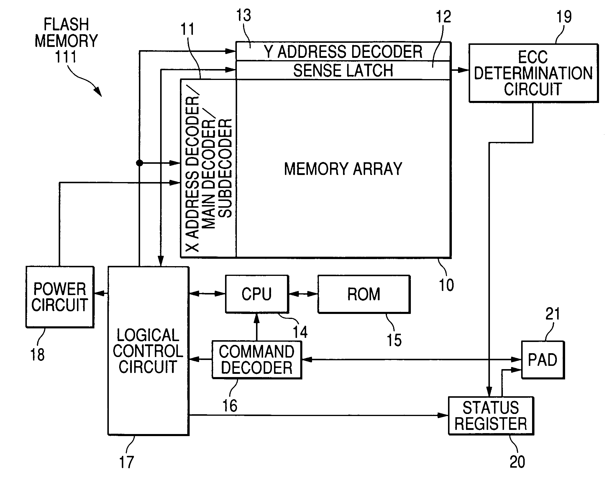
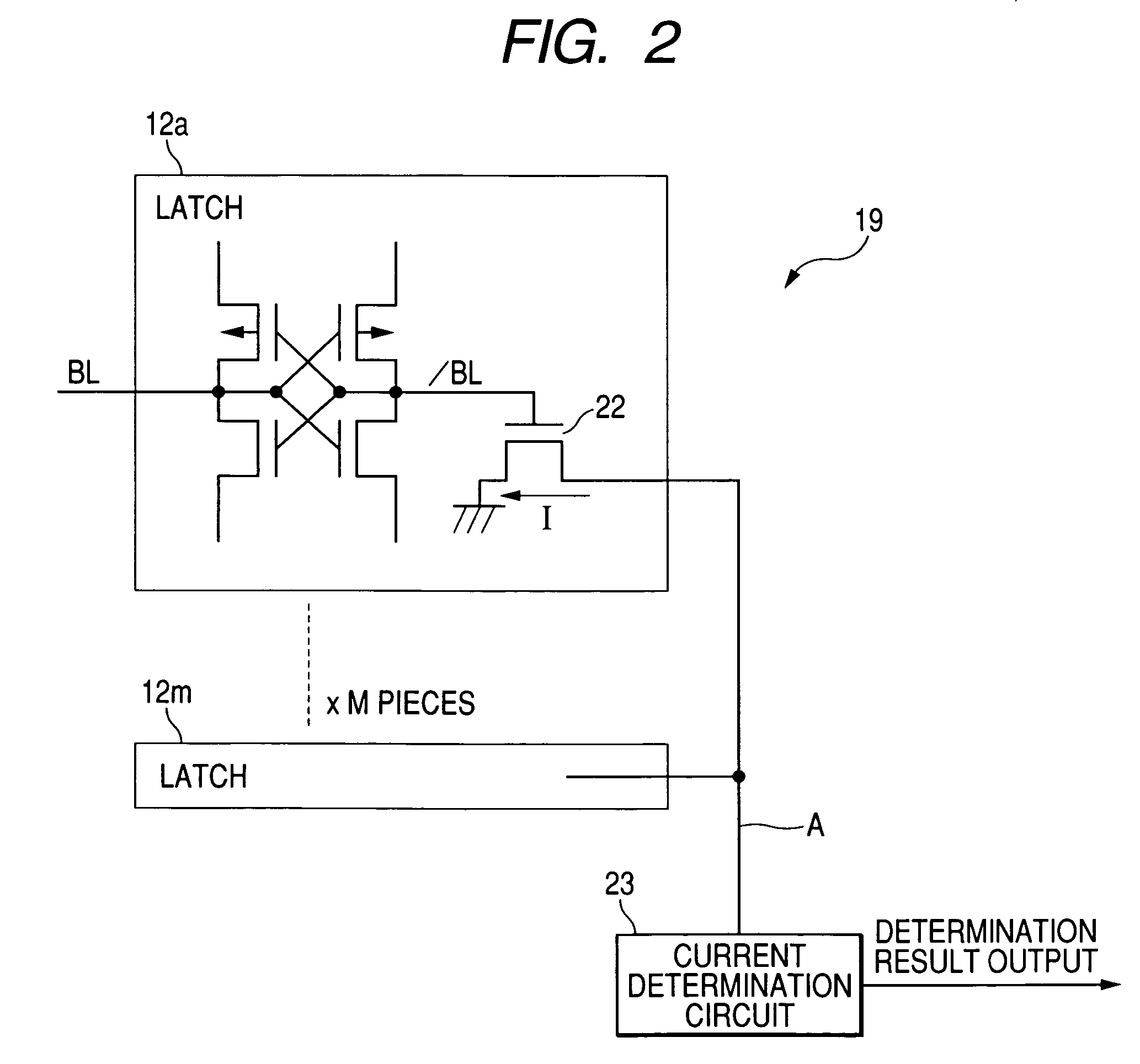
[0032]FIG. 1 is a block diagram showing the configuration of a nonvolatile memory according to a first embodiment of the present invention. FIG. 2 is a drawing showing the configuration of an ECC determination circuit in a nonvolatile memory of the first embodiment. FIGS. 3 and 4 are drawings showing a current determination circuit in the ECC determination circuit. FIG. 5 is a drawing showing the bit configuration of a status register. FIGS. 6 and 7 are drawings showing the flow of write operation. FIGS. 8 and 9 are drawings showing the flow of write operation of multi-level memory cells. FIGS. 10A and 10B are explanatory drawings showing the number of error bits of multi-level memory cells.

[0033]Referring to FIG. 1, an example of the configuration of nonvolatile memory according to the first embodiment will be described. A nonvolatile memory of the present embodiment, which is, for example, a flash memory 111, comprises a memory array 10 including plural nonvolatile memory cells, a...

second embodiment

[0063]FIG. 11 is a block diagram showing the configuration of a memory card of a second embodiment of the present invention. FIG. 12 is a drawing showing an example of a write flow in the memory card of the second embodiment. FIG. 13 is a drawing showing the flow of writing by a controller. FIG. 14 is a drawing showing another example of a write flow in the memory card.

[0064]Referring to FIG. 11, a description will be made of an example of the configuration of the memory card of the second embodiment. A memory card 110 of the second embodiment includes the flash memory 111 of the first embodiment, a controller 112, a host I / F (interface) 113, and the like. The flash memory 111 includes the ECC determination circuit 19 (error correction determination part) and the like. The controller 112 includes an ECC (error correction propriety determination part) 114 and the like. The flash memory 111 and the controller 112, and the controller 112 and the host I / F 113 are respectively connected....


PUM


Abstract

To provide a technique which enables a load on a controller to be reduced by rapidly detecting n-bit errors during writing / erasing on a chip in ECC in a nonvolatile memory. A flash memory of the present invention, which is a nonvolatile memory that includes plural electrically erasable and writable nonvolatile memory cells and performs write-and-verify processing in a write operation on the nonvolatile memory cells, includes an ECC determination circuit that counts the number of bits of write error detected in the write-and-verify processing, and outputs the information, and a status register for holding pass / fail information of the write operation and the information about the number of bits of write error outputted from the ECC determination circuit.

Description

CROSS REFERENCE TO RELATED APPLICATION[0001]The present application claims priority from Japanese patent application No. 2004-225271 filed on Aug. 2, 2004, the content of which is hereby incorporated by reference into this application.BACKGROUND OF THE INVENTION[0002]The present invention relates to a nonvolatile memory and a memory card including the memory, and more particularly to a technique operatively applied to the detection and correction (ECC) of write / erase bit errors of the nonvolatile memory.[0003]As a technology studied by the inventors, in a write operation on a nonvolatile memory such as a flash memory, verify processing is performed to determine whether the threshold voltage of memory cell reaches an expected value. In the verify processing, generally, writing and verifying are repeated until all the bits to be written pass. A write error of even one bit during the write operation is handled as a write error. To save the write error, a technique for detecting and cor...

Claims


Application Information

Patent Timeline
Patent Type & Authority Patents(United States)
IPC IPC(8): G11C29/00
CPCG06F11/1068G11C16/3454G11C11/5621G11C16/34G11C29/00
Inventor NODA, SATOSHIKOZAKAI, KENJIMATSUSHITA, TORUJONO, YUSUKE
Owner RENESAS ELECTRONICS CORP
Why Eureka
Try Eureka