Radiation detection device, scintillator panel, method of making the same, making apparatus, and radiation image pick-up system

a technology of radiation detection device and scintillator panel, which is applied in the direction of x/gamma/cosmic radiation measurement, radioation controlled devices, instruments, etc., can solve the problems of unsolved problems, inability to completely remove the huge splash, and inability to solve the problems described in known examples, etc., to achieve the effect of enhancing the quality of the radiation detection devi

Inactive Publication Date: 2008-01-01
CANON KK
View PDF50 Cites 35 Cited by
  • Summary
  • Abstract
  • Description
  • Claims
  • Application Information

AI Technical Summary

Benefits of technology

[0016]Therefore, an object of the present invention is to provide a scintillator in which there is not any irregularity on the surface of a scintillator layer and in which an abnormal growth portion such as splash existing inside the scintillator layer has been controlled to be very small, and a radiation detection device using the scintillator, thereby further enhancing quality of the radiation detection device.

Problems solved by technology

In the above-described method, it is difficult to completely remove the huge splash, a part of the splash is left on a scintillator surface, and accordingly problems described in known examples cannot be completely solved.
Moreover, even when any splash is not left on the scintillator surface, an abnormal growth portion such as a huge splash exists inside a scintillator layer, and therefore problems have remained unsolved such as drop of luminance and deterioration of resolution with respect to X-rays in a region where the abnormal growth portion exists, although the problems by the abnormal growth portion inside the scintillator layer have not been described in the known example.

Method used


Image

  • Radiation detection device, scintillator panel, method of making the same, making apparatus, and radiation image pick-up system
  • Radiation detection device, scintillator panel, method of making the same, making apparatus, and radiation image pick-up system
  • Radiation detection device, scintillator panel, method of making the same, making apparatus, and radiation image pick-up system

Examples


first embodiment

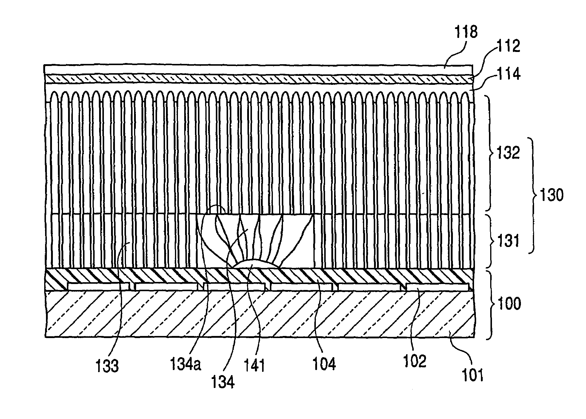
[0038]In Embodiment 1, the present invention is carried out as a radiation detection device and a method of making the device in a case where CsI:Tl (scintillator layer) is vapor-deposited directly on a photoelectric conversion panel (sensor panel) (referred to also as “direct vapor deposition type”).

[0039]The radiation detection device shown in FIG. 1 has: a photoelectric conversion panel 100; a scintillator layer 130 constituted of CsI:Tl formed by direct vapor deposition on the photoelectric conversion panel 100; a protective layer 114 formed on the scintillator material 130; a reflective layer 112 constituted of an aluminum thin film; and a protective layer 118.

[0040]The photoelectric conversion panel 100 shown in FIG. 1 comprises: a glass substrate 101; a photoelectric conversion element portion 102 constituted of a photo sensor and a thin-film transistor (TFT) using amorphous silicon (a-Si); and a protective layer 104 formed of silicon nitride and the like to protect the photo...

second embodiment

[0061]FIG. 4, FIGS. 5A to 5C show Embodiment 2. In Embodiment 2, the present invention is carried out as a radiation detection device and a method of making the device in a case where CsI:Tl is vapor-deposited on a substrate to form a scintillator panel, and the scintillator panel is bonded to a photoelectric conversion panel (referred to also as “laminated type”).

[0062]FIG. 4 shows a cross-sectional structure of the radiation detection device of Embodiment 2.

[0063]The radiation detection device shown in FIG. 4 has: a photoelectric conversion panel (sensor panel) 100; and a scintillator panel (fluorescent plate) 110.

[0064]The photoelectric conversion panel 100 comprises: a glass substrate 101; a photoelectric conversion element portion 102 constituted of a photo sensor and a thin-film transistor (TFT) using amorphous silicon; and a protective layer 104 formed of silicon nitride and the like to protect the photoelectric conversion element portion 102.

[0065]The scintillator panel 110 ...

third embodiment

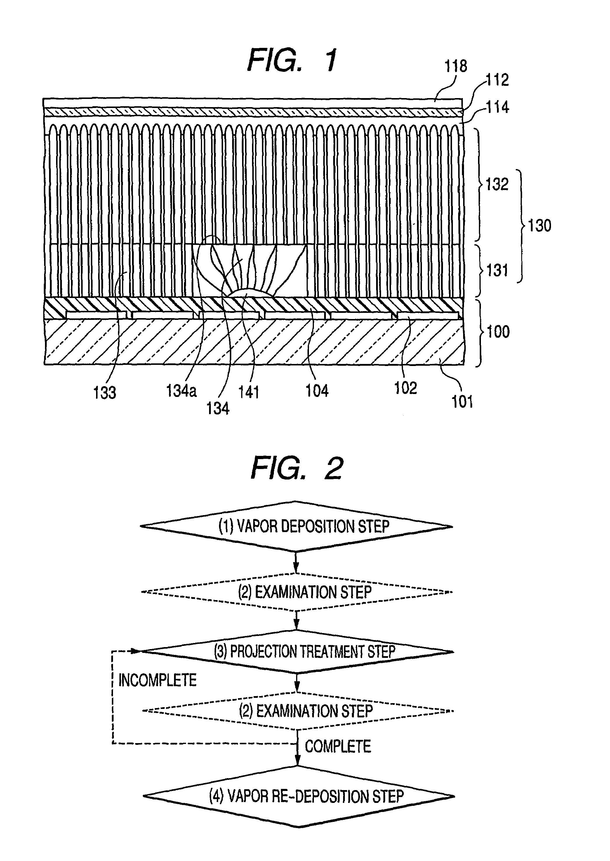
[0085]FIG. 6 shows Embodiment 3. The present embodiment shows an example in which the projection treatment during the vapor deposition is performed with respect to a second scintillator layer 132 in the same manner as in a first scintillator layer 131, and a third scintillator layer 137 is newly vapor-deposited again after the treatment. When abnormal growth portions 136 generated in the second scintillator layer 132 grow into crystals, and projections are formed on the surface of the second scintillator layer, a projection treatment step during the vapor deposition is performed in the same manner as in the first scintillator layer 131, the third scintillator layer 137 is newly vapor-deposited again after the treatment, and accordingly the surface can be flattened. When the scintillator layer is multilayered, and a thickness per layer of the scintillator layer is reduced in this manner, the projections that would be generated by the abnormal growth portions 136 are reduced, and it i...


PUM


Abstract

There are provided a scintillator (130) comprising a structure in which a plurality of scintillator layers (131, 132, 135) having columnar crystal structures are stacked with, and a radiation detection device using the scintillator. There are also provided a scintillator (130) comprising a structure in which a plurality of scintillator layers (131, 132, 135) and light-transmitting intermediate layers (138, 139) disposed among the plurality of scintillator layers (131, 132, 135) are alternately stacked with, and a radiation detection device using the scintillator. Accordingly, it is possible to control the scintillator layer in such a manner as to reduce irregularities on the surface of the scintillator layer, and reduce an abnormal growth portion such as a splash existing inside the scintillator layer. Therefore, a radiation detection device can be obtained which has high reliability, high resolution, and small correction error of a digital image.

Description

TECHNICAL FIELD[0001]The present invention relates to a radiation detection device for use in medical or analytical radiation image pick-up, a method of making the device, and a radiation detection system. It is to be noted that in the present description, electromagnetic waves such as X-rays and g-rays are assumed to be included in radiations.[0002]Radiation detection devices each constituted of a radiation sensitive sheet having a scintillator layer for converting X-rays into light, and a radiation film having a photosensitive layer have heretofore been used generally in X-ray photography.[0003]However, in recent years, radiation detection devices have been developed each having a two-dimensional detector comprising a scintillator constituted of a scintillator layer, a photoelectric conversion element using amorphous silicon (a-Si), and a thin-film transistor for a switch. This radiation detection device has been proposed as a flat panel detector (FPD), and is a photographing devi...

Claims


Application Information

Patent Timeline
Patent Type & Authority Patents(United States)
IPC IPC(8): G01T1/20G01T1/202H01L27/14H01L27/146H01L31/0232H01L31/18
CPCG01T1/2018G01T1/202H01L27/14618H01L27/14663H01L31/02322H01L31/18H01L2924/0002G01T1/2006H01L2924/00
Inventor OKADA, SATOSHITAMURA, TOMOYUKI
Owner CANON KK
Why Eureka
Try Eureka