Method for manufacturing a multi-layered thin film for use as an anode in a lithium secondary battery
a lithium secondary battery and multi-layer technology, applied in the direction of cell components, final product manufacturing, sustainable manufacturing/processing, etc., can solve the problems of failure to completely discharge, poor managability, damage to the device, etc., and achieve the effect of improving the charging/discharging cycle characteristics
- Summary
- Abstract
- Description
- Claims
- Application Information
AI Technical Summary
Benefits of technology
Problems solved by technology
Method used
Image
Examples
example 1
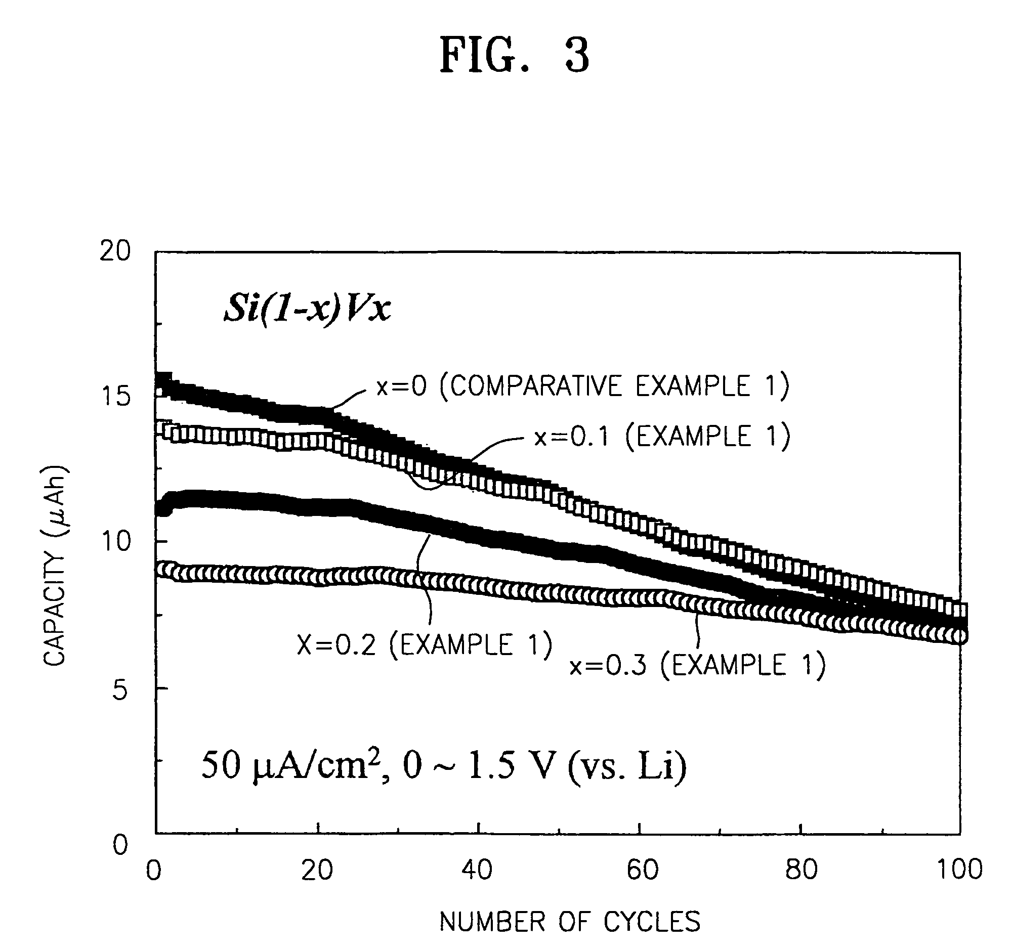
[0054]Various components of a thin film, that is, Si, V and Ag targets each having a diameter of 2 inches, were sequentially deposited on a copper (Cu) substrate to prepare a Cu / V (200 Å) / Si-V (300 Å) / Ag (50 Å) thin film for an anode.
[0055]During sputtering, the initial degree of vacuum was first adjusted to 2×10⁻⁶ torr or less, a vanadium (V) layer was then deposited to a thickness of 200 Å at rf power of 50 W under the condition of Ar gas induced at 5 mTorr operating pressure and 10 sccm flow rate, and Si and V were co-sputtered on the resultant product to a thickness of 300 Å to prepare a single-layered Si—V film (sometimes also called a “layer” throughout the specification). Ag was then deposited on the Si—V film to a thickness of 50 Å.
[0056]In order to adjust the contents of Si and V in the single-layered Si—V film, the rf power applied to the V target in the range of 0 to 100 W was varied, while fixing the rf power applied to the Si target to 200 W, thereby manufacturing thin ...
examples 2-4
[0065]Thin films for an anode were manufactured in the same manner as in Example 1, except that each Si0.7M0.3 layer (300 Å) was formed using Mn, Ti and Zr as metals (M) in an Si-M layer as anode active material layers, instead of V, respectively.
[0066]Lithium secondary batteries employing the single-layered films as anodes were manufactured, and FIGS. 6A through 6C show cycle characteristics thereof. Evaluation of cycle characteristics of these thin films for an anode was made by repeating at least 50 cycles of charging and discharging. Referring to FIGS. 6A through 6C, in the case of single-layered films with Mn, Ti and Zr added, like in the case of the single-layered Si—V film, deterioration of anode active materials due to volumetric expansion and shrinkage of Si was considerably reduced, thereby greatly improving cycle characteristics compared to the case of Comparative Example 1. The initial discharge capacity of each single-layered film was maintained without a considerable r...
example 5
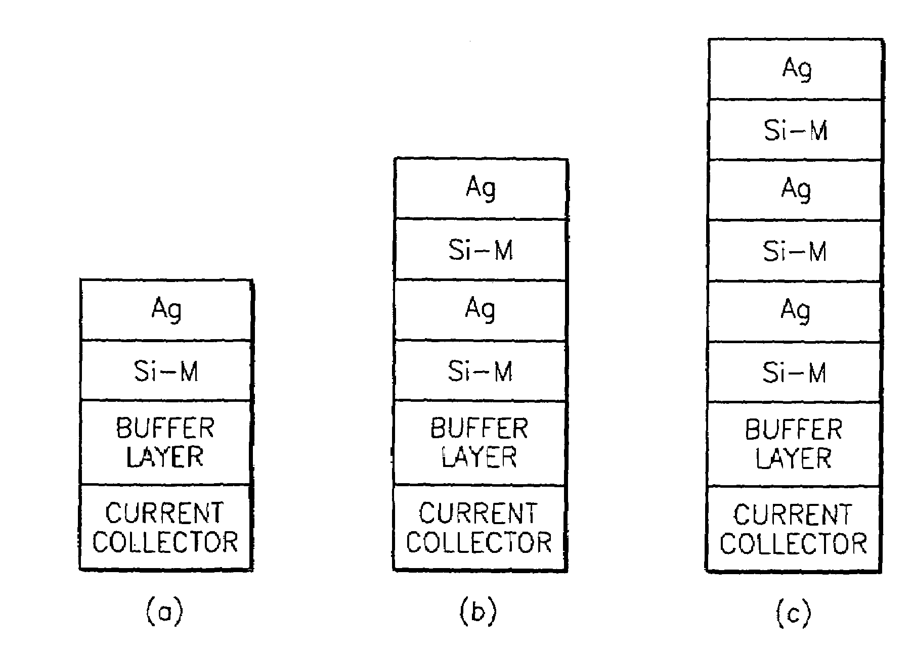
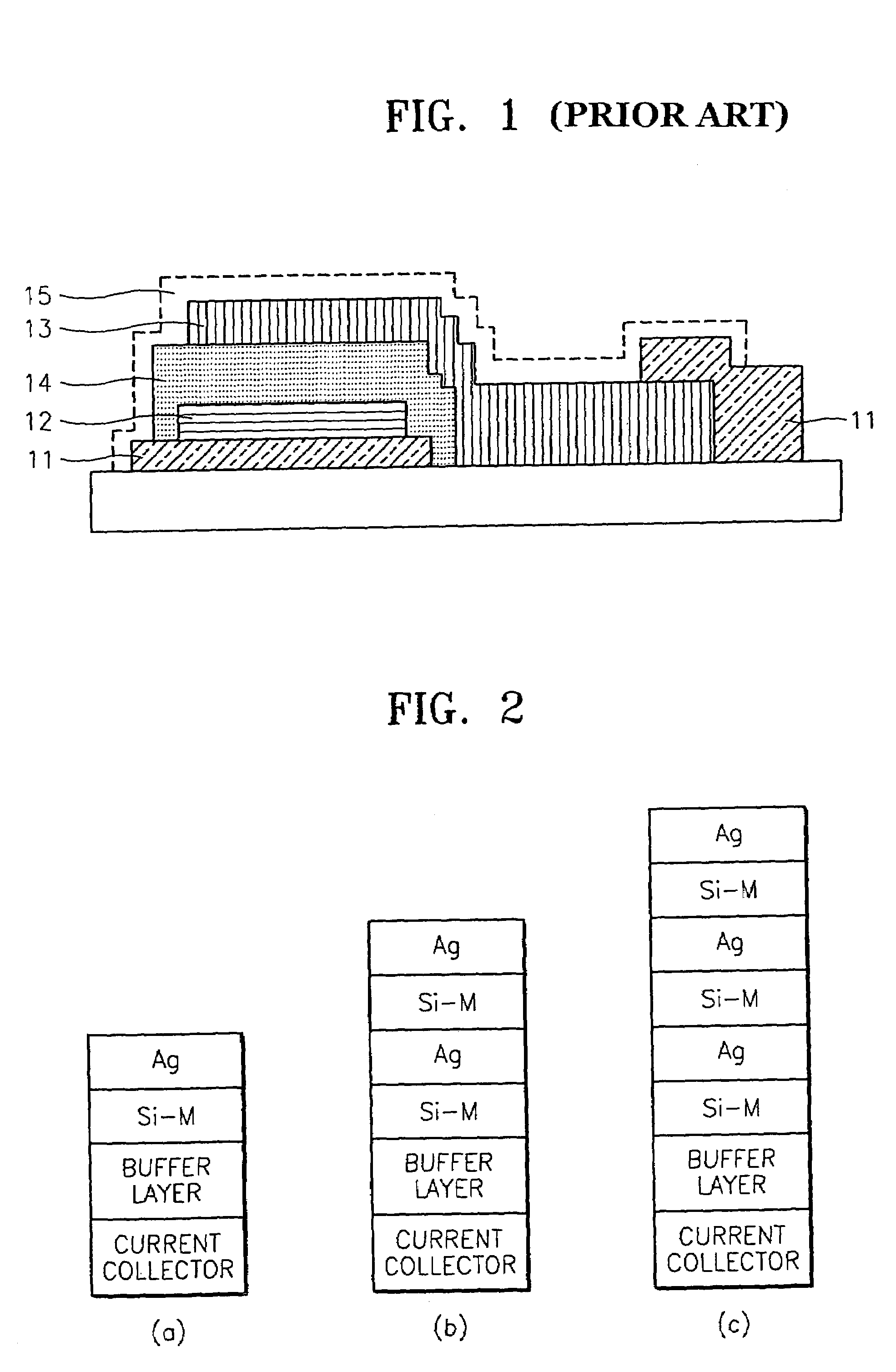
[0068]Various components of a thin film for an anode, that is, Si, V and Ag targets each having a diameter of 2 inches, were sequentially deposited on a Cu substrate to prepare thin films for an anode having the structures shown in Table 1. During sputtering, the initial degree of vacuum was first adjusted to 2×10⁻⁶ torr or less, a vanadium (V) layer was then deposited to a thickness of 200 Å at rf power of 50 W under the condition of Ar gas induced at 5 mTorr operating pressure and 10 sccm flow rate, and an Ag layer and an Si—V layer alternately deposited on the resultant product. The Ag layer was deposited between Si—V layers to a thickness of 50 Å at a dc voltage of 270 V with a current of 30 mA, and the Si—V layer having the same composition as in Example 1, that is, the Si0.7V0.3 layer, was deposited to a thickness of 150 Å
[0069]
TABLE 1SampleLayered structure of anode active materialMSB-1Cu / V (200 Å) / (Si-V) / AgMSB-2Cu / V (200 Å) / (Si-V) / Ag / (Si-V) / AgMSB-3Cu / V (200 Å) / (Si-V) / Ag / (Si-...
PUM
| Property | Measurement | Unit |
|---|---|---|
| thickness | aaaaa | aaaaa |
| thickness | aaaaa | aaaaa |
| melting point | aaaaa | aaaaa |
Abstract
Description
Claims
Application Information


