Substrate for display device having a protective layer provided between the pixel electrodes and wirings of the active matrix substrate, manufacturing method for same, and display device

a technology of active matrix substrate and substrate, which is applied in the direction of optics, instruments, transistors, etc., can solve the problems of display point defects, and achieve the effects of high aperture ratio, high yield and high display quality

Active Publication Date: 2008-01-15
SHARP KK
View PDF16 Cites 14 Cited by
  • Summary
  • Abstract
  • Description
  • Claims
  • Application Information

AI Technical Summary

Benefits of technology

[0023]The present invention is provided in view of the above described current state, and an object of the invention is to provide a substrate for a display device that makes it possible to obtain a display device of a high display quality with a high yield by preventing short-circuiting between a pixel electrode and wirings, such as a scan line or a signal line, particularly when a substrate for a display device having high definition and a high aperture ratio is manufactured, and a manufacturing method for the same, as well as a display device that uses such a substrate.
[0024]The present inventors have, in a variety of manners, examined substrates for display devices having high definition and high aperture ratios and which make it possible to obtain a display device having a high display quality with a high yield, and have found that defect of film, such as peeling of an (upper) interlayer insulation film located beneath a pixel electrode may occur in a region where a wiring, such as a scan line (gate bus line) or a signal line (source bus line), and a pixel electrode overlap in a plane (region where the two overlap as viewed in the direction perpendicular to the surface of the substrate) in the conventional configuration of a substrate. The inventors focused on the occurrence of defects of leakage in such a case, since a gate insulator or the like in the defect portion is etched by using the (upper) interlayer insulation film as a mask for etching, and wirings, such as the scan line or the signal line (source bus line) is exposed, and then the exposed wiring and the pixel electrode make contact with each other by film forming and patterning of the pixel electrode. That is to say, when such a leakage occurs between the wiring and the pixel electrode, a potential written in a pixel cannot be maintained, leading to a point defect in the display. Therefore, inventors have found that providing a protective layer above the wiring such as the scan line and the signal line (source bus line) as a protective layer against etching can prevent contact between the pixel electrode and the wiring, leading to prevention of a defect of leakage caused by such short-circuiting. The inventors have found that, for example, a pattern of a semiconductor layer to form a switching element is disposed on a region where the scan line and the pixel electrode overlap on a plane, and thereby, this semiconductor layer pattern works as a protective film against etching, even when the interlayer insulation film is peeled, and thus, electrical leakage between the pixel electrode and the scan line can be prevented without increasing the number of steps in the manufacturing process for a substrate, and it becomes possible to provide a display device such as a liquid crystal display device having a high definition and a high aperture ratio with a high yield, and in this manner, means that can completely solve the above described problem are provided, leading to the completion of the present invention.

Problems solved by technology

That is to say, when such a leakage occurs between the wiring and the pixel electrode, a potential written in a pixel cannot be maintained, leading to a point defect in the display.

Method used


Image

  • Substrate for display device having a protective layer provided between the pixel electrodes and wirings of the active matrix substrate, manufacturing method for same, and display device
  • Substrate for display device having a protective layer provided between the pixel electrodes and wirings of the active matrix substrate, manufacturing method for same, and display device
  • Substrate for display device having a protective layer provided between the pixel electrodes and wirings of the active matrix substrate, manufacturing method for same, and display device

Examples


embodiment 1

[0123]Embodiment 1, which is one embodiment of the present invention, is described below, with reference to FIGS. 1 to 4.

[0124]And according to the present embodiment, an active matrix substrate for a liquid crystal display device is described as a specific example of a substrate for a display device.

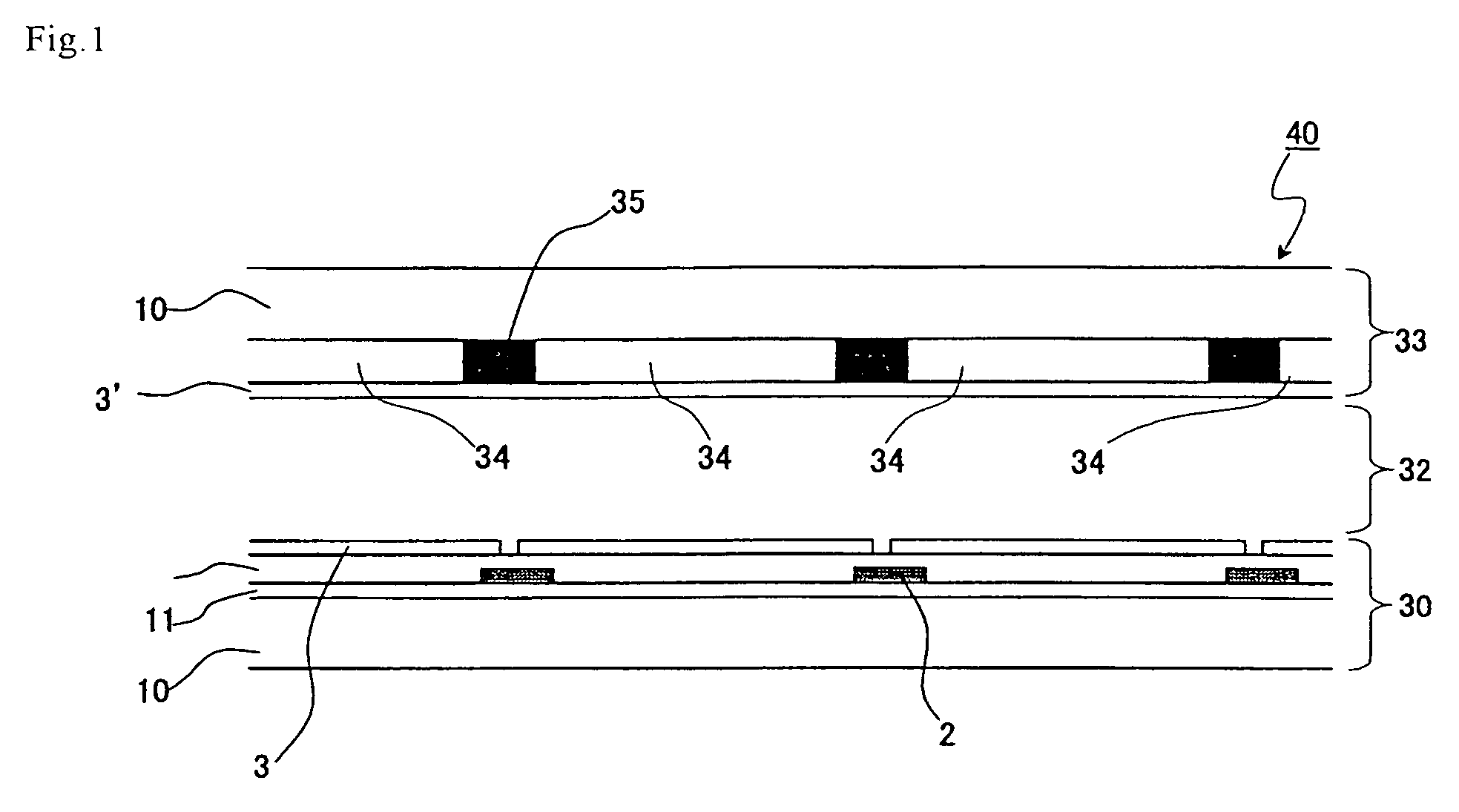
[0125]FIG. 1 is a schematic cross sectional diagram showing one example of the configuration of a liquid crystal display device according to the present invention.

[0126]As shown in FIG. 1, the liquid crystal display devices 40 has the active matrix substrate (substrate for a display device) 30 and the facing substrate 33 having the color filter 34 and the light blocking film 35, and these substrates sandwich the liquid crystal layer 32. The liquid crystal layer 32 is placed between the orientation film (not shown) of the facing substrate 33, and the orientation film (not shown) of the active matrix substrate 30.

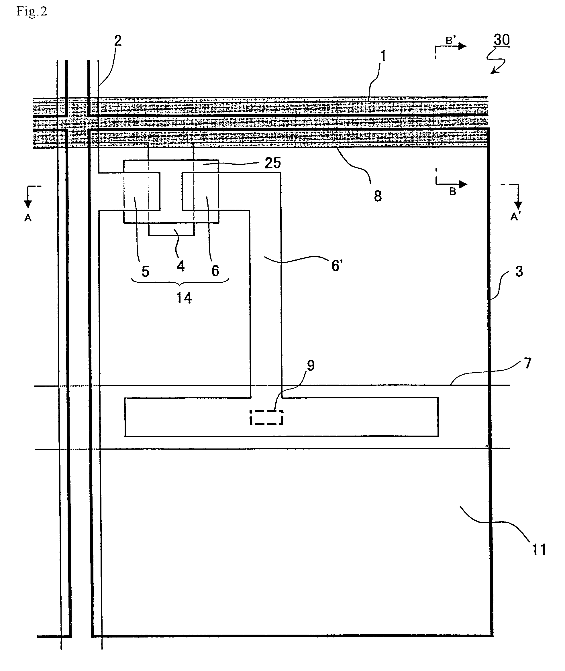
[0127]FIG. 2 is a schematic plan diagram showing one pixel in active matrix ...

embodiment 2

[0146]Embodiment 2, which is another embodiment according to the present invention, is described below, with reference to FIGS. 5 to 7. For the purpose of convenience of description, the same symbols are attached to members having the same functions as those shown in the drawings of Embodiment 1, and the descriptions thereof are omitted.

[0147]According to Embodiment 2, a protective layer is formed together with a semiconductor layer to form a switching element (TFT), and after that, is separated from the semiconductor layer of the switching element, so as to have a configuration not overlapping the source lines. An active matrix substrate (substrate for a display device) according to Embodiment 2, where such a protective layer (hereinafter referred to also as a protective semiconductor layer), is provided, is described with reference to FIGS. 5 to 7.

[0148]FIG. 5 is a schematic plan diagram showing one element in the active matrix substrate 30 according to the present invention. FIG....

embodiment 3

[0158]Embodiment 3, which is another embodiment according to the present invention, is described below, with reference to FIGS. 8 to 10. And for the purpose of convenience of description, the same symbols are attached to members having the same functions as those shown in the drawings concerning Embodiments 1 and 2, and the descriptions thereof are omitted.

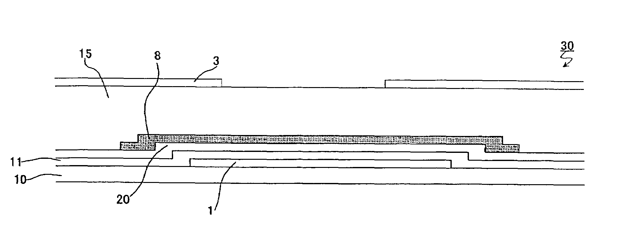
[0159]The configuration according to Embodiment 3 is characterized in that a protective semiconductor layer is disposed least in portions where the gate lines (scan lines) and the pixel electrode overlap as viewed in the direction perpendicular to the surface of the insulating substrate in the configuration of Embodiment 2. The active matrix substrate 30 according to Embodiment 3 where such a protective semiconductor layer is provided is described with reference to FIGS. 8 to 10.

[0160]FIG. 8 is a schematic plan diagram showing one pixel in the active matrix substrate 30 according to the present invention.

[0161]FIG. 9 is a cross se...


PUM

PropertyMeasurementUnit
thicknessaaaaaaaaaa
compositionaaaaaaaaaa
capacitanceaaaaaaaaaa

Abstract

The present invention provides the substrate for a display device, comprising a scan line, a signal line and a switching element on an insulating substrate, and further comprising an interlayer insulation film and a pixel electrode, the switching element is provided at an intersection of the scan line and the signal line, and have a gate electrode connected to the scan line, a source electrode connected to the signal line, and a drain electrode connected to the pixel electrode, the interlayer insulation film has a contact hole for connecting the drain electrode of the switching element to the pixel electrode, and a protective layer is provided above the scan line and / or the signal line in the substrate for a display device.

Description

REFERENCE TO RELATED APPLICATION[0001]The Nonprovisional application claims priority under 35 U.S.C. § 119(a) on Patent Application No. 2004-154506 filed in Japan on May 25, 2004, the entire contents of which are hereby incorporated by reference.BACKGROUND OF THE INVENTION[0002]1. Field of the Invention[0003]The present invention relates to a substrate for a display device, a manufacturing method for the same, and a display device. More specifically, the present invention relates to a substrate for a display device that can be applied to a liquid crystal display device and the like, a manufacturing method for the same, and a display device that has such a substrate.[0004]2. Description of the Related Art[0005]At present, liquid crystal display devices have characteristics such as compact, thin, lightweight, and low power consumption, and have been widely used in a variety of electronic apparatuses. In particular, active matrix type liquid crystal display devices (liquid crystal disp...

Claims


Application Information

Patent Timeline
Patent Type & Authority Patents(United States)
IPC IPC(8): G02F1/1343G02F1/1333G02F1/136G02F1/1362G02F1/1368H01L21/336H01L21/768H01L23/522H01L29/786
CPCG02F1/136227G02F2001/136231G02F2201/50G02F1/136231G02F1/136
Inventor TSUBATA, TOSHIHIDEENDA, KENJI
Owner SHARP KK
Why Eureka
Try Eureka