Plasma display panel and method of driving the same

Inactive Publication Date: 2008-01-15
LG ELECTRONICS INC
View PDF6 Cites 3 Cited by
  • Summary
  • Abstract
  • Description
  • Claims
  • Application Information

AI Technical Summary

Benefits of technology

[0026]Accordingly, the present invention has been made in view of the above problems, and it is an object of the present invention to

Problems solved by technology

In the conventional 3-electrode structure, however, it is impossible to form a wide positive column having good discharge efficiency because the distance between the scan electrode Y and the sustain electrode Z is narrow.
Due to this, the conventional 3-electrode structure has a disadvantage that the discharge efficiency is low.
However, since the particle size of Xe is significantly larger than those of Ne, the path of charges is limited if the amount of Xe is high.
In other words, the increase in the amount of Xe results in i

Method used


Image

  • Plasma display panel and method of driving the same
  • Plasma display panel and method of driving the same
  • Plasma display panel and method of driving the same

Examples


first embodiment

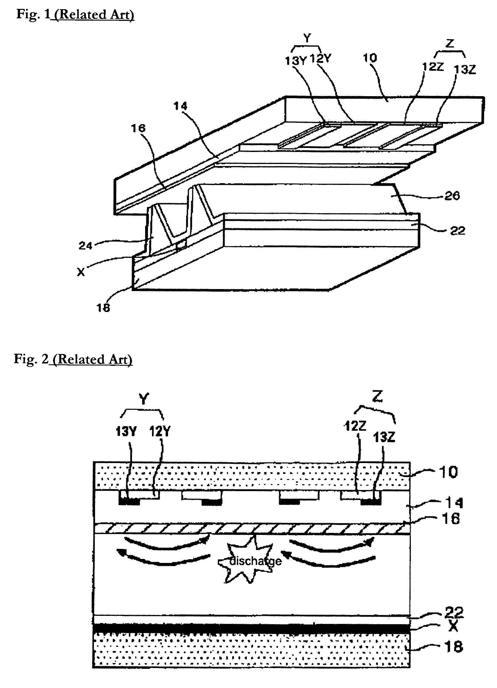
[0073]FIG. 6 is a cross-sectional view of a PDP according to an embodiment of the present invention.

[0074]Referring to FIG. 6, a discharge cell of a 3-electrode AC sheet discharge type PDP using a positive column according to a first embodiment of the present invention includes a scan electrode Y and a sustain electrode Z formed on an upper substrate 110, and an address electrode X formed on a lower substrate 118. Each of the scan electrode Y and the sustain electrode Z includes transparent electrodes 112Y and 112Z, and metal bus electrodes 113Y and 113Z having a line width smaller than a line width of the transparent electrodes 112Y and 112Z and formed in an edge region of one side of the transparent electrode.

[0075]The transparent electrodes 112Y and 112Z are usually formed of indium-tin-oxide (hereinafter, referred to as “ITO”) on the upper substrate 10. The metal bus electrodes 113Y and 113Z are formed on the transparent electrodes 112Y and 112Z usually using a metal such as chr...

second embodiment

[0102]A PDP according to a first embodiment of the present invention is a structure using he positive column. In this structure, the distance between the scan electrode and the sustain electrode is set wider than the distance between the scan electrode and the address electrode. Thus, the sustain voltage Vs is a little high compared to the conventional structure. It can be said that this problem is basically derived from the relationship d>L in FIG. 7. Accordingly, the first embodiment and another embodiment for lowering the sustain voltage Vs a little in a safe manner will be described.

[0103]FIGS. 12a and 12b show electrode structures according to a second embodiment of the present invention.

[0104]Referring to FIGS. 12a and 12b, the electrode structure includes a scan electrode Y and a sustain electrode Z which are formed in parallel to each other on a upper substrate, an address electrode X formed on a lower substrate so that the address electrode X intersects the scan electrode Y...

third embodiment

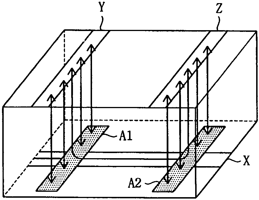
[0108]FIGS. 13a and 13b show an electrode structure according to a third embodiment of the present invention.

[0109]Referring to FIGS. 13a and 13b, the electrode structure includes a scan electrode Y and a sustain electrode Z, which are formed in parallel to each other on a upper substrate, an address electrode X formed on a lower substrate so that the address electrode X intersects the scan electrode Y and the sustain electrode Z, and auxiliary electrodes A11 and A12 formed on the address electrode X at places where the scan electrode Y and the sustain electrode Z and the address electrode X intersect.

[0110]In the above, the auxiliary electrodes A11 and A12 have a width wider than that of the scan electrode Y and the sustain electrode Z. Furthermore, these auxiliary electrodes A11 and A12 may be formed on the part of only one side of the scan electrode Y and the sustain electrode Z and may be formed so that they extend only in one direction of each electrode.


PUM


Abstract

A plasma display panel is disclosed. More particularly, the present invention relates to a plasma display panel, which can improve discharge stability as well as brightness and efficiency. The plasma display panel according to the present invention includes transparent electrodes (ITO electrodes) spaced in parallel to each other at a predetermined distance; and metal electrodes each formed on the transparent electrodes (ITO electrodes) in parallel to the transparent electrodes (ITO electrodes) so that the respective transparent electrodes (ITO electrodes) are inclined toward the side where the transparent electrodes face.

Description

BACKGROUND OF THE INVENTION[0001]1. Field of the Invention[0002]The present invention relates to a plasma display panel, and more particularly, to a plasma display panel and method for driving the same, which can increase discharge efficiency.[0003]2. Background of the Related Art[0004]A plasma display panel (hereinafter, referred to as “PDP”) displays images including characters or graphics since fluorescent material is emitted by ultraviolet rays of 147 nm occurring when inert mixed gases of He+Xe, Ne+Xe, He+Ne+Xe, etc. are discharged. It is easy for this PDP to be made thin and large. The PDP also provides an improved picture quality due to recent advanced technology. In particular, in a 3-electrode AC sheet discharge PDP, wall charges are accumulated on the surface of the PDP upon the discharge of the PDP and electrodes are protected from sputtering occurring due to the discharge. Therefore, the 3-electrode AC sheet discharge PDP advantageously has a low-voltage driving and a lo...

Claims


Application Information

Patent Timeline
IPC IPC(8): H01J17/49G09G3/20G09G3/288G09G3/291G09G3/292G09G3/293G09G3/294G09G3/298H01J11/22H01J11/24H01J11/28H01J11/34
CPCG09G3/2983G09G3/2986H01J11/12H01J11/32G09G2310/066G09G2320/0228H01J2211/323
Inventor CHOI, SUNG CHUNKANG, JUNGWONSONG, JUN WEON
Owner LG ELECTRONICS INC
Why Eureka
Try Eureka