Method and apparatus for driving a thin film transistor liquid crystal display

a technology of thin film transistors and liquid crystal displays, which is applied in the direction of instruments, computing, electric digital data processing, etc., can solve the problems of deterioration of picture images displayed on the lcd screen, scale down of picture image quality,

Active Publication Date: 2008-01-15
SAMSUNG ELECTRONICS CO LTD
View PDF6 Cites 19 Cited by
  • Summary
  • Abstract
  • Description
  • Claims
  • Application Information

AI Technical Summary

Benefits of technology

[0022]Another exemplary embodiment of the present invention is directed to a method of eliminating offsets of driving voltage in a TFT-LCD. The TFT-LCD may include a plurality of amplifiers, each amplifier having first and second input ports and generating a panel driving voltage of a positive or negative polarity corresponding to a input digital signal. In the method, a panel driving voltage is applied to a given pixel of a liquid crystal panel in response to a clock signal. The polarity of the applied panel driving voltage may be changed in response to a polarity control signal. A switch control signal, synchronized to the clock signal, may be generated to switch the first and second input ports of each of the plurality of amplifiers.

Problems solved by technology

The stripe phenomenon results in degradation scale in the quality of picture images displayed on the LCD screen.
Thus, the quality of picture images displayed on an LCD screen may deteriorate.

Method used


Image

  • Method and apparatus for driving a thin film transistor liquid crystal display
  • Method and apparatus for driving a thin film transistor liquid crystal display
  • Method and apparatus for driving a thin film transistor liquid crystal display

Examples


Embodiment Construction

[0035]Hereinafter, exemplary embodiments of the present invention will be described in greater detail with reference to the accompanying drawings, in which preferred embodiments of the invention are shown. The same reference numerals in different drawings represent the same elements.

[0036]The exemplary embodiments of the present invention are directed to an TFT-LCD source driver circuit capable of improving picture quality of a TFT-LCD device by preventing a stripe phenomenon caused by an offset, i.e., differences among the voltages output from a plurality of amplifiers in the TFT-LCD source driver circuit. Additionally, exemplary embodiments of the present invention are directed to a method of driving voltage so as to eliminate differences among voltages output from a plurality of amplifiers in an apparatus or circuit such as a TFT-LCD source driver circuit, for example.

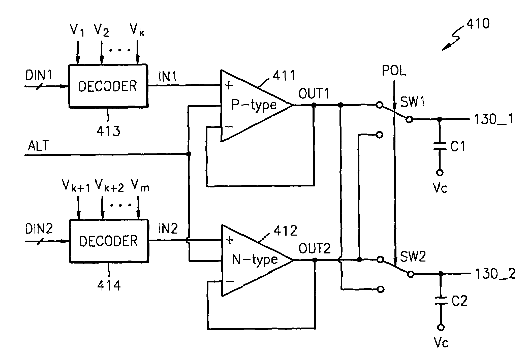
[0037]FIG. 4 is a block diagram of a source driver integrated circuit 400 according to an exemplary embodiment of...


PUM

PropertyMeasurementUnit
voltageaaaaaaaaaa
grey scale voltageaaaaaaaaaa
output voltagesaaaaaaaaaa

Abstract

A method and apparatus is described that may be capable of improving picture quality of a TFT-LCD device, to prevent occurrence of a stripe phenomenon caused by an offset, i.e., differences among the voltages output from a plurality of amplifiers in a TFT-LCD source driver circuit. The method and apparatus may eliminate differences among voltages output from a plurality of amplifiers in a circuit such as a TFT-LCD source driver circuit. In the method, a panel driving voltage may be applied to a given pixel of a liquid crystal panel in response to a clock signal. The polarity of the applied panel driving voltage may be changed in response to a polarity control signal, and a switch control signal may be generated based on the polarity control signal. The switch control signal may be applied to switch first and second input ports of each of the plurality of amplifiers.

Description

PRIORITY STATEMENT[0001]This application claims the priority of Korean Patent Application No. 2002-77032, filed on Dec. 5, 2002, in the Korean Intellectual Property Office, the disclosure of which is incorporated herein in its entirety by reference.BACKGROUND OF THE INVENTION[0002]1. Field of the Invention[0003]The present invention relates to a thin film transistor (TFT)-liquid crystal display (LCD) panel driving circuit capable of preventing stripes from occurring on a TFT-LCD panel.[0004]2. Description of the Related Art[0005]TFT-LCD display devices are widely used in laptops and computer monitors. Circuits for driving TFT-LCD panels may be generally divided into gate driver circuits and source driver circuits.[0006]FIG. 1 is a circuit diagram of a prior art TFT-LCD device. Referring to FIG. 1, a typical TFT-LCD device 100 includes a liquid crystal panel 105, a source driver circuit 110, and a gate driver circuit 120.[0007]Each pixel 150 of the liquid crystal panel 105 is compris...

Claims


Application Information

Patent Timeline
Patent Type & Authority Patents(United States)
IPC IPC(8): G09G3/36G09G5/00G02F1/133G09G3/20
CPCG09G3/3688G09G3/3614G09G3/36
Inventor CHOI, CHANG-HWE
Owner SAMSUNG ELECTRONICS CO LTD
Why Eureka
Try Eureka