Array connector having improved electrical characteristics and increased signal pins with decreased ground pins

a technology of electrical characteristics and signal pins, applied in the direction of coupling device connections, coupling contact member materials, coupling protection earth/shielding arrangements, etc., can solve the problems of reducing the number of signal pins that can be present in the connector, increasing the size of the connector, and affecting the electrical characteristics of the connector, so as to improve the electrical characteristics, reduce cross-talk, and improve the electrical characteristics

Active Publication Date: 2008-01-29
SAMTEC
View PDF13 Cites 84 Cited by
  • Summary
  • Abstract
  • Description
  • Claims
  • Application Information

AI Technical Summary

Benefits of technology

[0014]In order to overcome the unsolved problems of the prior art described above, preferred embodiments of the present invention provide an electrical connector having the same or reduced size, and which includes a much higher number of signal pins and a much lower number of ground pins or ground blades, while greatly improving the electrical characteristics thereof, such as improved electrical characteristics, greatly reduced cross-talk, increased bandwidth, improved impedance matching, and greatly reduced EMI emissions from the connector.

Problems solved by technology

The use of so many pins as ground pins or the use of ground blades in between adjacent signal pins may increase the size of the connector, may decrease the number of signal pins that can be present in the connector, or both.
These problems are especially difficult in a differential pair array connector where differential signals are passed through the connector.
In addition, the ground pins or ground blades must be arranged so as to surround the differential signal pairs because of disadvantageous broadside coupling between adjacent differential signal pairs.
This is referred to as disadvantageous broadside coupling.
As is clear from the above description, one of the unsolved problems of prior art array connectors is how to increase signal pin density without increasing the size of the connector or decreasing the quality of the electrical characteristics of the connector, and without complicating the arrangement of ground pins or ground blades.
Conventional array connector design dictates that the number of ground pins or ground blades cannot be minimized or eliminated without a concomitant increase in cross-talk and deterioration of electrical characteristics of the connector.
No suitable solution to this problem has been developed.
Another problem that occurs with such array connectors of the prior art is the use of so many ground pins requires a much more complex design and connection process for the PCB upon which the connector will be mounted and used.
Because so many ground pins must be used in the pin field, a much greater number of PCB layers, traces, and vias must be used to properly route and connect the ground pins, which makes the PCB design and manufacturing process much more difficult, as well as, making the connection of the array connector to the PCB more difficult.
Also, with the increased number of PCB layers, traces, and vias, there is much greater impedance mismatching, increased cross-talk, and greatly increased manufacturing complexity and cost for the PCB used with the connector.
Also, the contact and terminal solder termination and retention features are non-uniform and different for each connector.
This greatly increases the complexity and cost of manufacturing such connectors and related PCBs.
That is, a standard pin arrangement and construction of an array connector cannot be adapted to various unique array connector designs.

Method used


Image

  • Array connector having improved electrical characteristics and increased signal pins with decreased ground pins
  • Array connector having improved electrical characteristics and increased signal pins with decreased ground pins
  • Array connector having improved electrical characteristics and increased signal pins with decreased ground pins

Examples


Embodiment Construction

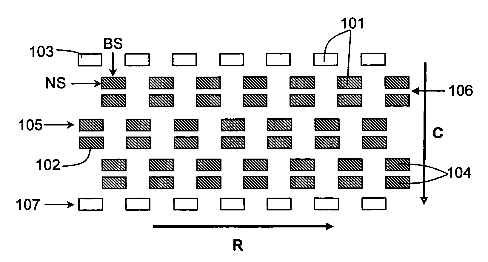
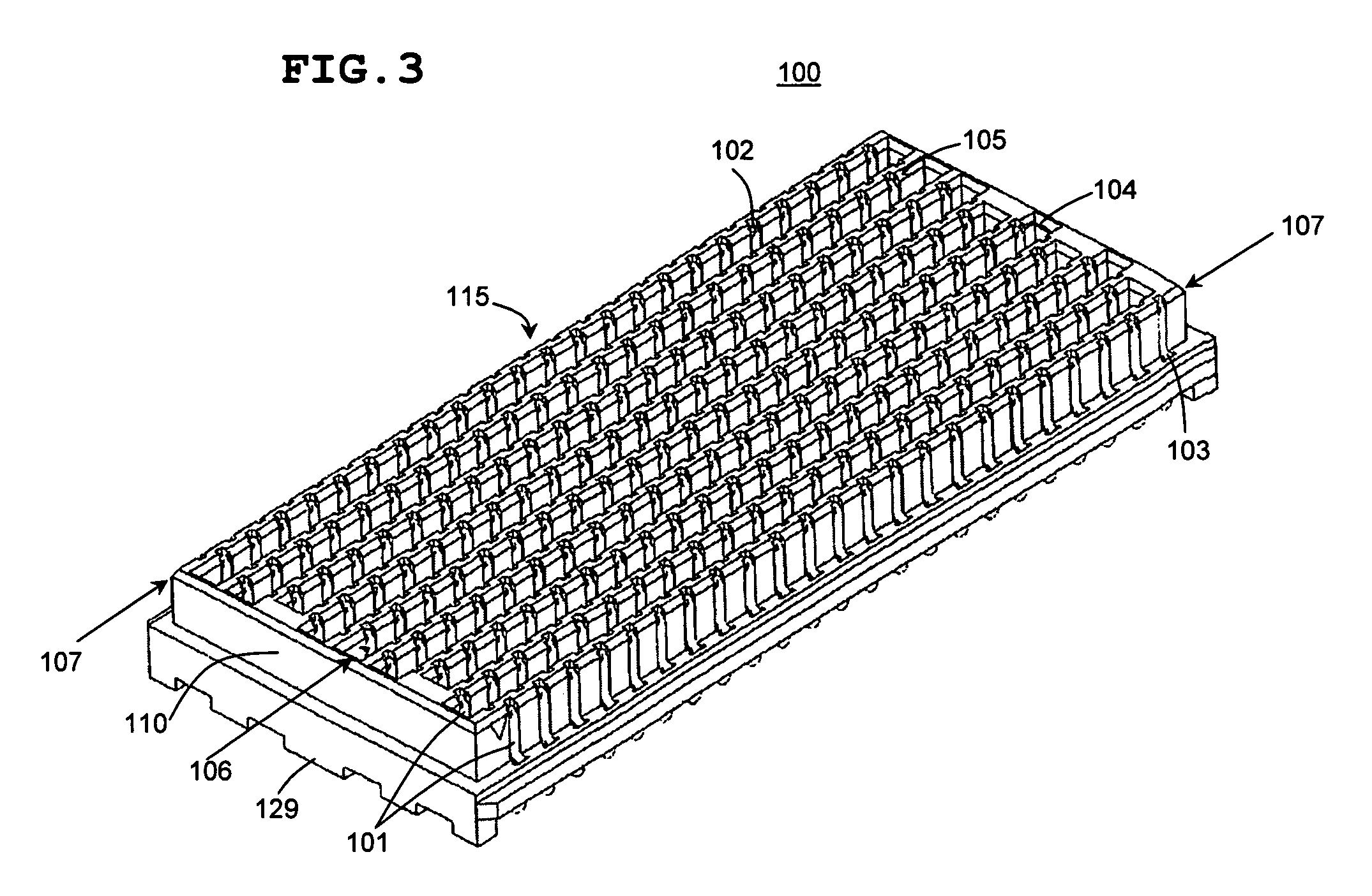
[0046]FIGS. 2, 3, 4, and 5 show an electrical connector 100 according to a preferred embodiment of the present invention. The electrical connector 100 includes a connector body 110 having a plurality of rows of pins 101.

[0047]It should be noted that the preferred embodiment shown in FIGS. 2-5 is preferably a differential pair array connector, but other connectors such as a single ended array connector or other types of connectors are possible with the present invention.

[0048]As seen in FIG. 2, an electrical connector 100 includes a plurality of the pins 101, which include signal pins 102 and ground pins 103, described in more detail below.

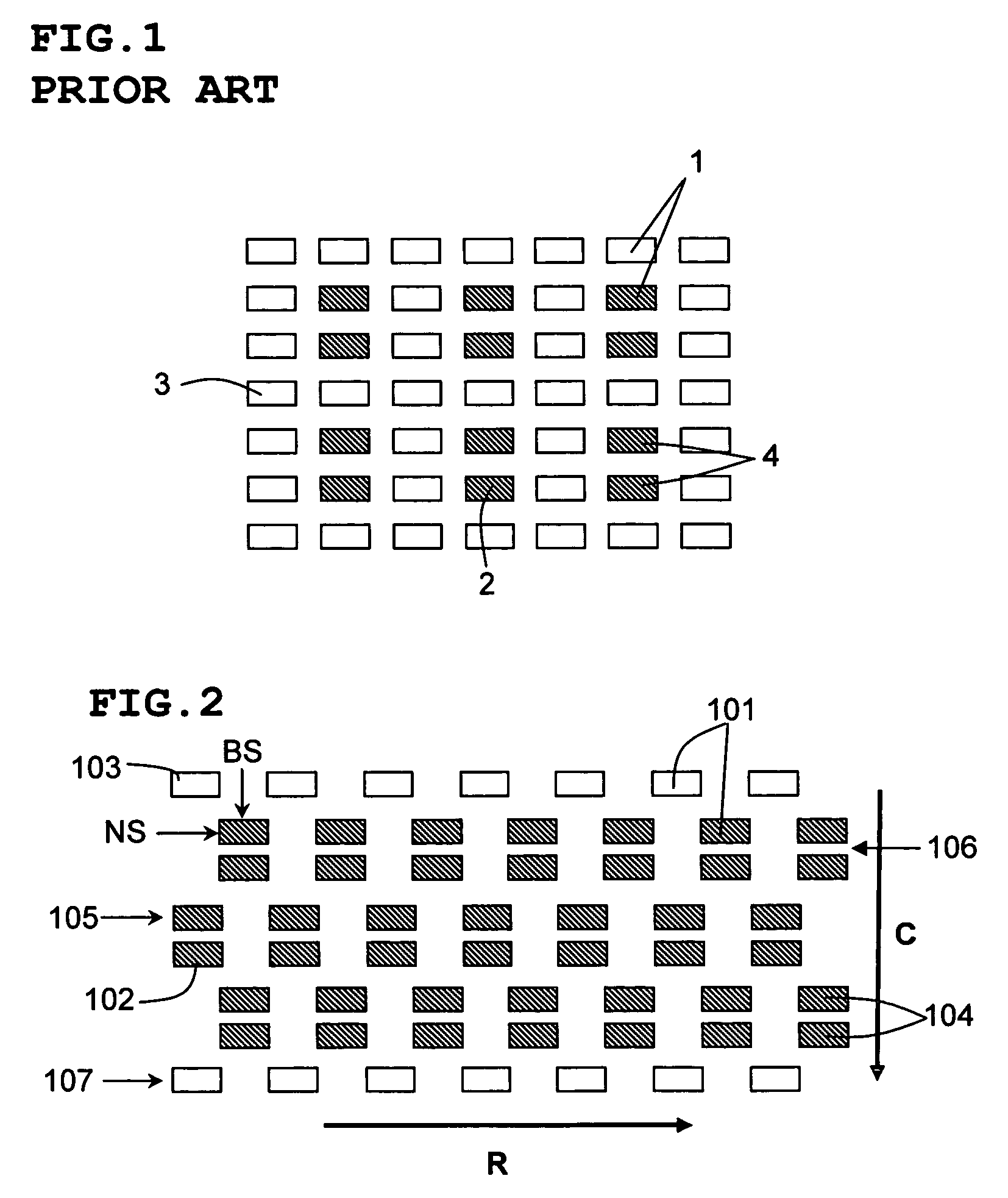
[0049]As is readily understood from FIG. 2, the various pins 101 have a staggered and stretched arrangement throughout the array of pins 101 due to varying distances between the pins, as compared with the uniformly spaced arrangement of the pins 2 and 3 in Prior Art FIG. 1. That is, as seen in FIG. 1, the distance between each of the pins 1 is the ...


PUM


Abstract

An electrical connector includes a connector body, a plurality of rows and columns of conductive pins disposed along the length direction and the width direction of the connector body so as to form an array of signal pins located in a pin field, at least two rows of ground pins arranged along at least two sides of the pin field, with no ground pins being arranged in the pin field or between adjacent signal pins. The signal pins are arranged in a stretched pitch and / or staggered configuration to minimize cross-talk and maximize signal pin density and signal-to-ground ratio.

Description

BACKGROUND OF THE INVENTION[0001]1. Field of the Invention[0002]The present invention relates to electrical connectors. More specifically, the present invention relates to array connectors, which can be a single-ended array connector or a differential pair array connector, which uses far fewer ground pins or blades and has a greater number of signal pins and achieves significantly improved electrical characteristics.[0003]2. Description of the Related Art[0004]It is known to provide an electrical connector, such as a board-to-board mezzanine connector, having a regular array of signal pins in a pin field. The signal pins must be surrounded by ground pins or ground blades or planes, which are provided both within the pin field and surrounding the pin field in order to prevent cross-talk between adjacent signal pins and to prevent EMI emissions from the pin field to the outside of the connector. For example, US 2003 / 0027439 A1, to Johnescu et al., teaches surrounding each of the signa...

Claims


Application Information

Patent Timeline
Patent Type & Authority Patents(United States)
IPC IPC(8): H01R13/648H01R4/66H01R11/00H01R12/16H01R13/658
CPCH01R13/6471H01R13/6587H01R13/6473
Inventor MONGOLD, JOHN A.FERRY, JULIAN J.KUVSHINIKOV, TODD J.
Owner SAMTEC
Why Eureka
Try Eureka