

Low noise amplifier for wideband tunable matching
a wideband tunable matching and low noise technology, applied in the direction of amplifier modification, amplifier combination, amplifier modification to reduce noise influence, etc., can solve the problems of difficult system integration, increased complexity and power consumption, and low noise amplifiers having the common gate structure not being used widely. , to achieve the effect of optimizing performan
- Summary
- Abstract
- Description
- Claims
- Application Information
AI Technical Summary
Benefits of technology
Problems solved by technology
Method used
Image

Examples
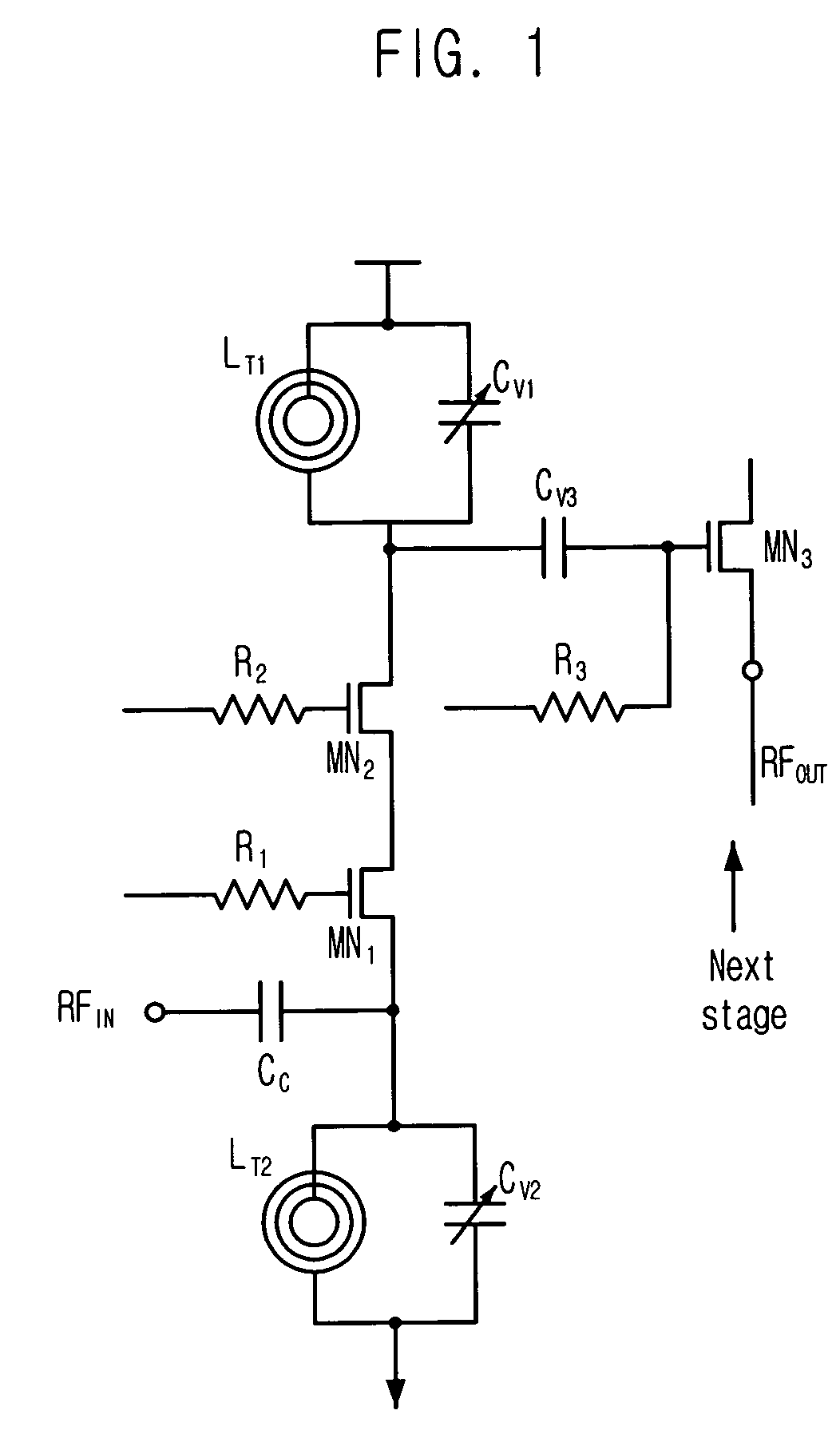
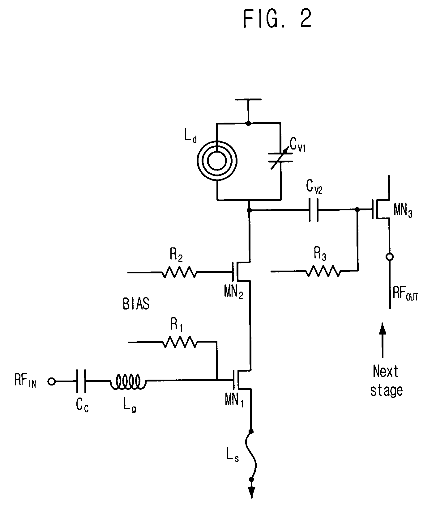
first embodiment
[0027]FIG. 3 is a circuit diagram of a low noise amplifier having an inductively degenerated common source structure in accordance with the present invention.
[0028]Referring to FIG. 3, the low noise amplifier includes an inductor Lg, a MOS transistor MN1, and a variable capacitor Csc. The inductor Lg has one terminal connected to an input terminal receiving a signal RFin and the other terminal connected to a ground. The MOS transistor MN1 has a gate connected to the inductor Lg, a source connected to an inductor Ls, and a drain transmitting a signal. The variable capacitor Csc is connected between the source and gate of the MOS transistor MN1 and changes an input matching frequency of the input terminal.
[0029]A capacitor Cc is provided for removing a DC component transmitted through the input terminal. A resistor R1 is provided for biasing the gate of the MOS transistor MN1.
[0030]The variable capacitor Csc may be a capacitor that is continuously varied in response to a control signa...
second embodiment
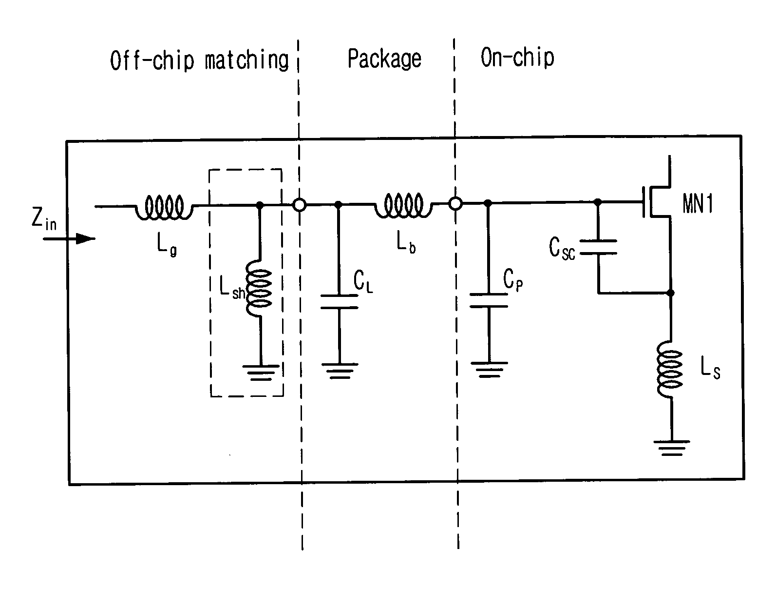
[0055]FIG. 5 is a circuit diagram of a low noise amplifier having an inductively degenerated common source structure in accordance with the present invention. In FIG. 5, the parasitic capacitance applied at the input terminal of the low noise amplifier is equivalently removed using a shunt inductor Lsh.
[0056]Referring to FIG. 5, the low noise amplifier includes an inductor Lg, an inductor Ls, a MOS transistor MN1, a variable capacitor CSC, and a shunt inductor Lsh. The inductor Lg has one terminal connected to an input terminal receiving a signal. The inductor Ls has one terminal connected to a ground. The MOS transistor MN1 has a gate connected to the inductor Lg, a source connected to the other terminal of the inductor Ls, and a drain transmitting a signal. The variable capacitor CSC is connected between the source and gate of the MOS transistor MN1 so as to vary the input impedance at the input terminal. The shunt inductor Lsh is connected between the gate of the MOS transistor M...
third embodiment
[0066]FIG. 6 is a circuit diagram of a low noise amplifier having an inductively degenerated common source structure in accordance with the present invention. In FIG. 6, the parasitic capacitance applied at the input terminal of the low noise amplifier is removed using a shunt capacitor Csh.
[0067]Referring to FIG. 6, the low noise amplifier includes an inductor Lg, an inductor Ls, a MOS transistor MN1, a variable capacitor CSC, and a shunt capacitor Csh. The inductor Lg has one terminal connected to an input terminal receiving a signal. The inductor Ls has one terminal connected to a ground. The MOS transistor MN1 has a gate connected to the inductor Lg, a source connected to the other terminal of the inductor Ls, and a drain transmitting a signal. The variable capacitor CSC is connected between the source and gate of the MOS transistor MN1 so as to vary the input impedance at the input terminal. The shunt capacitor Csh is connected between the input terminal and the ground and is r...
PUM
 Abstract
Description
Claims
Application Information