Switched capacitor circuit capable of minimizing clock feedthrough effect and having low phase noise and method thereof
a technology of switching capacitor and clock feedthrough, which is applied in the field of switching capacitor circuits, can solve the problems of undesired change in vco frequency and overall capacitance, and achieve the effect of minimizing the clock feedthrough effect and low phase nois
- Summary
- Abstract
- Description
- Claims
- Application Information
AI Technical Summary
Benefits of technology
Problems solved by technology
Method used
Image
Examples
first embodiment
[0032]FIG. 5 shows a switched capacitor circuit 500 according to the present invention. In FIG. 5, the switched capacitor circuit 500 includes a capacitor 502, a first switch element 504, and a precharge circuit 506. The precharge circuit 506 includes a second switch element 508, a precharge switch element 510, and a delay unit 512. The capacitor 502 is connected between the first oscillator node OSC_P and a node A. The first switch element 504 selectively connects node A to a second node, which is ground in this embodiment, according to a first control signal SW1. The precharge switch element 510 is coupled to a node D being a constant supply voltage of VDD in this embodiment. When the switched capacitor circuit 500 is turned off according to the first control signal SW1, the first switch element 504 disconnects node A from the ground. The precharge circuit 506 is coupled to node A for precharging node A to a precharge voltage for a predetermined period of time when the switched ca...
third embodiment
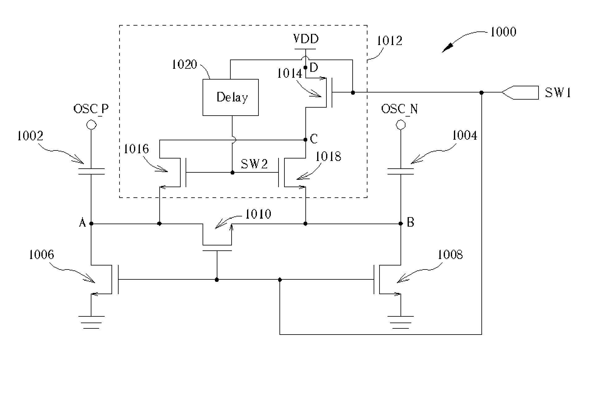
[0045]FIG. 12 shows a waveform diagram of the first control signal SW1, a second control signal SW2 outputted by the delay unit 1112, and the resulting voltage level at node A of the switched capacitor circuit 1100 according to the In this embodiment, when the switched capacitor circuit 1100 is switched off, the first control signal SW1 drops from a logic high value (VDD) to a logic low value (0V). The precharge switch element 1110 in the precharge circuit 1106 is thereby turned on at the same time that the first switch element 1104 is turned off according to the first control signal SW1. The second switch element 1108 continues to be turned on by the second control signal SW2, which is formed in the delay unit 1112 by delaying the first control signal SW1 by the predetermined time period T. In this way, the second switch element 1108 acts as a forward biased diode and node A is rapidly charged to a precharge voltage being VDD minus a voltage drop Vt across the second switch elemen...
second embodiment
[0055]In the present invention method and using FIG. 11 as an example, steps 1402 and 1404 further involve coupling the first positive node A to a third node C according to the second control signal SW2, providing a diode coupled between the first positive side node A and the third node C, coupling the third node C to the fourth node D according to the first control signal SW1; and generating the second control signal SW2. Wherein, the second control signal SW2 is the first control signal SW1 delayed by the predetermined time, and the second node{ground} (ground) is coupled to a constant voltage source at a first voltage level, the fourth node{VDD} D is coupled to a constant voltage source at a second voltage level. By ensuring a first voltage difference between the second voltage level and the value of the second control signal SW2 in an off-state is smaller than a second voltage difference between the first voltage level and the value of the second control signal SW2 in an onstate...
PUM
 Abstract
Description
Claims
Application Information


