Optical element and lighting device provided therewith

a technology of optical elements and lighting devices, which is applied in the direction of lighting and heating apparatus, printing, instruments, etc., can solve the problems of impracticality very large lens size, large lens size, complicated configuration, etc., and achieves simple configuration, low cost, and efficient condensation

Inactive Publication Date: 2008-02-19
KONICA MINOLTA OPTO
View PDF15 Cites 10 Cited by
  • Summary
  • Abstract
  • Description
  • Claims
  • Application Information

AI Technical Summary

Benefits of technology

[0033]In view of the problems described above, the present invention has been made, and it is an object of the invention to provide an optical element which can achieve efficient condensation at low costs and with simple configuration and also can achieve compactification with a small diameter of the optical element with respect to the size of a light emitting surface, and to a lighting device including this optical element.

Problems solved by technology

However, the solid-state light-emitting element has a large angle of divergence of light emitted from the light emitting surface, thus leading to an enormous lens size, when used in a conventional optical system, in attempt to achieve condensation with low loss.
In patent document 2, which employs refraction and total reflection to change the direction of a ray of light from the light source, light emitted from the light source reaches the total reflection surface after passing through the refracting surface, which results in complicated configuration.
In patent document 3, which employs the bulk-type lens in order to increase rays of light emitted forward of the light source, the size of the lens is impractically very large when a surface light source with a large diameter is used as a light source.
In patent document 4, in which the exit side surface of the optical element has very complicated configuration, the degree of difficulty in manufacturing is great, thus disadvantageously leading to cost increase and lower efficiency.
Therefore, an increase in the area of the light-emitting surface of the light-emitting element requires an increase in the maximum diagonal length of the top surface 102b, thus resulting in an increase in the diameter of the optical element, which fails to provide a compact optical element.
This requires a large inclination of the peripheral side surface 101 with respect to the optical axis, thus resulting in a large diameter of the optical element, which leads to failure to achieve compact configuration of the optical element.
In conclusion, the configuration of the optical elements suggested in patent documents 1 to 6 suffer, in efficiently condensing the light-emitting element (improving the directivity of a ray of light emitted from the light-emitting element), from: a problem of complicated form of the optical element, which leads to cost increase; and a problem of a large diameter of the optical element with respect to the size of the light emitting surface of the light-emitting element, which results in insufficient compactification.

Method used


Image

  • Optical element and lighting device provided therewith
  • Optical element and lighting device provided therewith
  • Optical element and lighting device provided therewith

Examples


first embodiment

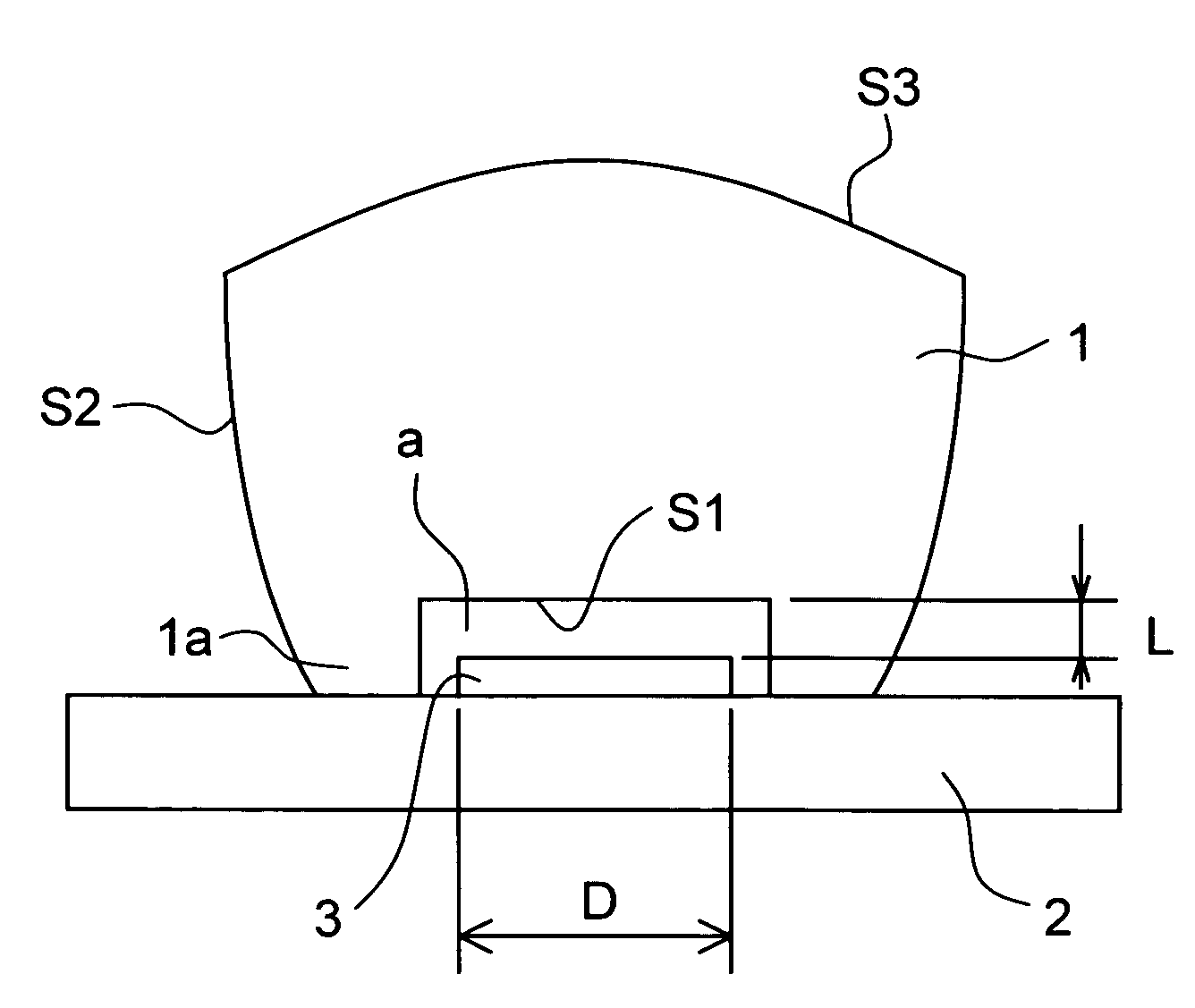
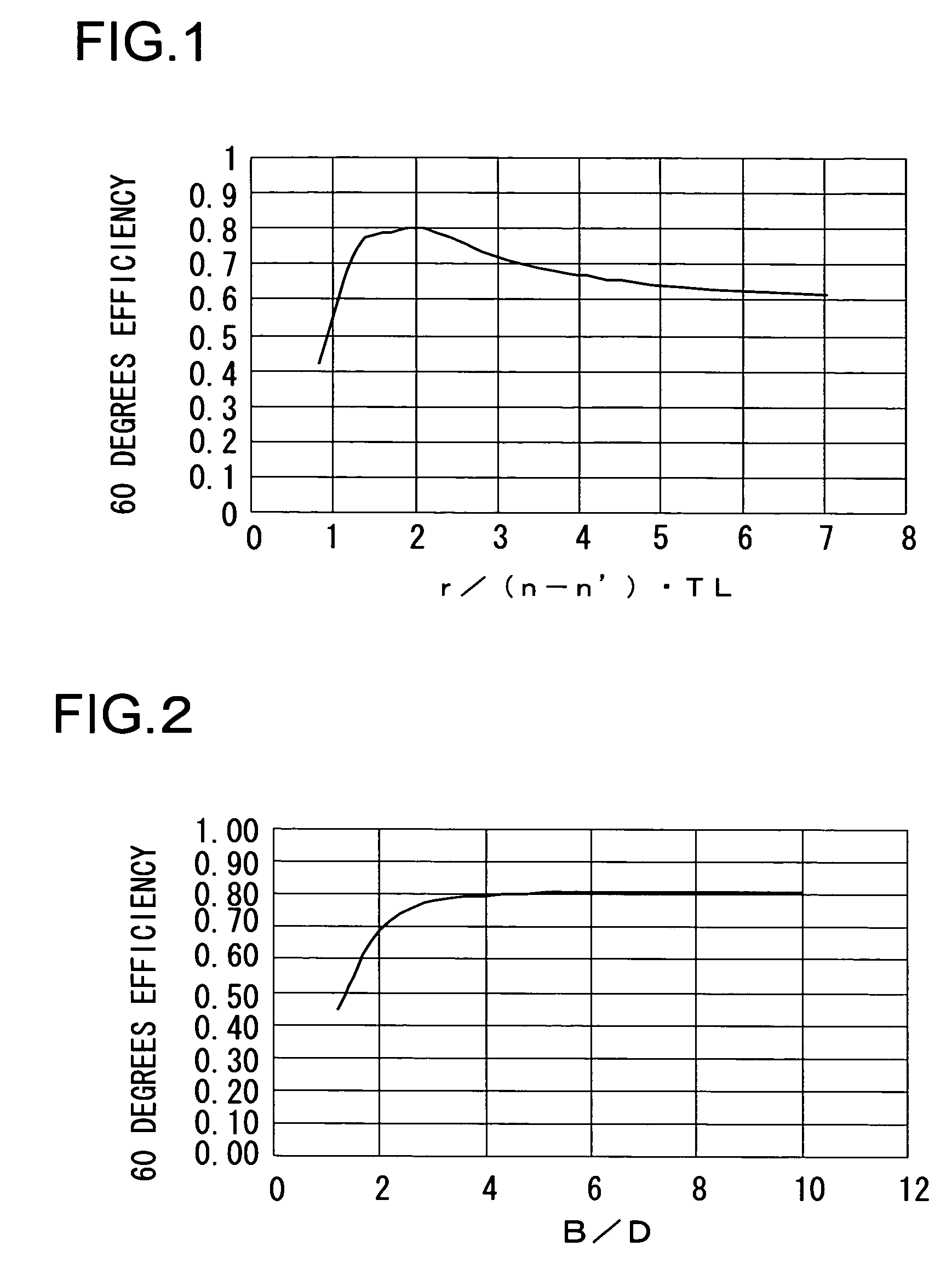
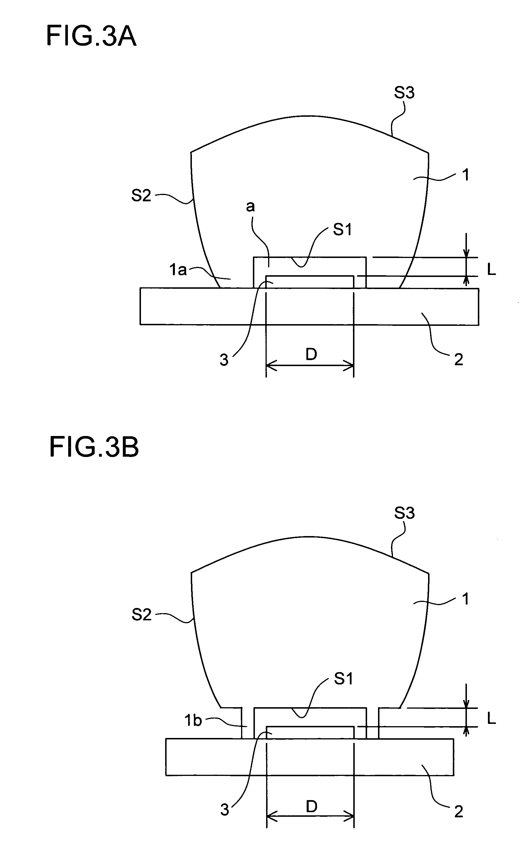
[0083]Hereinafter, one embodiment of the present invention will be described with reference to the accompanying drawings. The invention refers to an optical element which condenses in a predetermined direction light emitted from a light source having a widening surface form. This optical element has a first surface, a second surface, and a third surface. The first surface is an entrance surface formed of a flat surface where light emitted from the light source enters. The third surface is an exit surface from which light entering via the first surface exits and which is so formed as to be convexed on the light exit side. The second surface is a reflection surface which directs, to the third surface by total reflection, part of light entering via the first surface and which is so formed as to be convexed on the light entrance side. With the first surface disposed near the light source, light exiting from the light source enters the first surface, is totally reflected by the convexed ...

example 1

[0153]

Material: PMMARefractive index (d-line): 1.4914νd: 57.82[Effective[Z (mm)][CR (mm)][k]diameter (mm)]Light source (3)0INF0.0010First surface (S1)0.03INF0.0010Second surface (S2)−3.0954−1.0030surface apexThird surface (S3)29.03−500.0030surface apex

example 2

[0154]

Material: PolycarbonateRefractive index (d-line): 1.5834νd: 30.23[Effective[Z (mm)][CR (mm)][k]diameter (mm)]Light source (3)0INF0.0010First surface (S1)0.5INF0.0010Second surface (S2)−2.6254−1.0030surface apexThird surface (S3)29.5−400.0030surface apex


PUM


Abstract

An optical element that condenses light emitted from a light source has: an entrance surface where the light enters; an exit surface from which the light entering inside via the entrance surface; and a reflection surface that directs, to the exit surface by total reflection, part of the light entering the inside via the entrance surface. The reflection surface has an axis of symmetry of sixfold or higher-order-fold rotation. The optical element fulfills conditional formula: 0.3<a / b<1.4, where a denotes the maximum length of the exit surface in the direction perpendicular to the axis of symmetry; and b denotes a surface gap on the axis of symmetry between the entrance surface and the exit surface. As a result, an optical element can be provided which achieves highly efficient condensation at low costs and with simple configuration and also which achieves compactification by reducing the diameter of the optical element for the size of the light emitting surface.

Description

[0001]This application is based on Japanese Patent Application No. 2005-228995 filed on Aug. 8, 2005 and Japanese Patent Application No. 2006-118047 filed on Apr. 21, 2006, the contents of which are hereby incorporated by reference.BACKGROUND OF THE INVENTION[0002]1. Field of the Invention[0003]The present invention relates to an optical element suitable for a light source (light-emitting element), such as a light-emitting diode or the like, and a lighting device provided with such an optical element, and more specifically to an optical element suitable for improving the directivity of light (a ray of light) emitted from a light-emitting element and a lighting device provided with such an optical element.[0004]2. Description of the Prior Art[0005]In recent years, with an increase in the power of a semiconductor light-emitting element (solid-state light-emitting element), such as a light-emitting diode (LED) or the like, application of the solid-state light-emitting element to the il...

Claims


Application Information

Patent Timeline
Patent Type & Authority Patents(United States)
IPC IPC(8): G02B27/02F21V5/00F21V5/04F21V7/00G02B17/00H01L33/48
CPCH01L33/58G02B19/0028G02B19/0061H01L33/60
Inventor IKUNO, KEIKOKONNO, KENJI
Owner KONICA MINOLTA OPTO
Why Eureka
Try Eureka