Switching voltage regulator with an improved range of input voltage

a voltage regulator and input voltage technology, applied in the direction of power conversion systems, instruments, dc-dc conversion, etc., can solve the problems of finite physical time and the need for accumulation and depletion of charges, and achieve the effect of improving the range of input voltag

a voltage regulator and input voltage technology, applied in the direction of power conversion systems, instruments, dc-dc conversion, etc., can solve the problems of finite physical time and the need for accumulation and depletion of charges, and achieve the effect of improving the range of input voltag

US7339360B2Active Publication Date: 2008-03-04GLOBAL MIXED MODE TECH

Image

  • Switching voltage regulator with an improved range of input voltage
  • Switching voltage regulator with an improved range of input voltage
  • Switching voltage regulator with an improved range of input voltage

Examples


Embodiment Construction

[0024]The preferred embodiments according to the present invention will be described in detail with reference to the drawings.

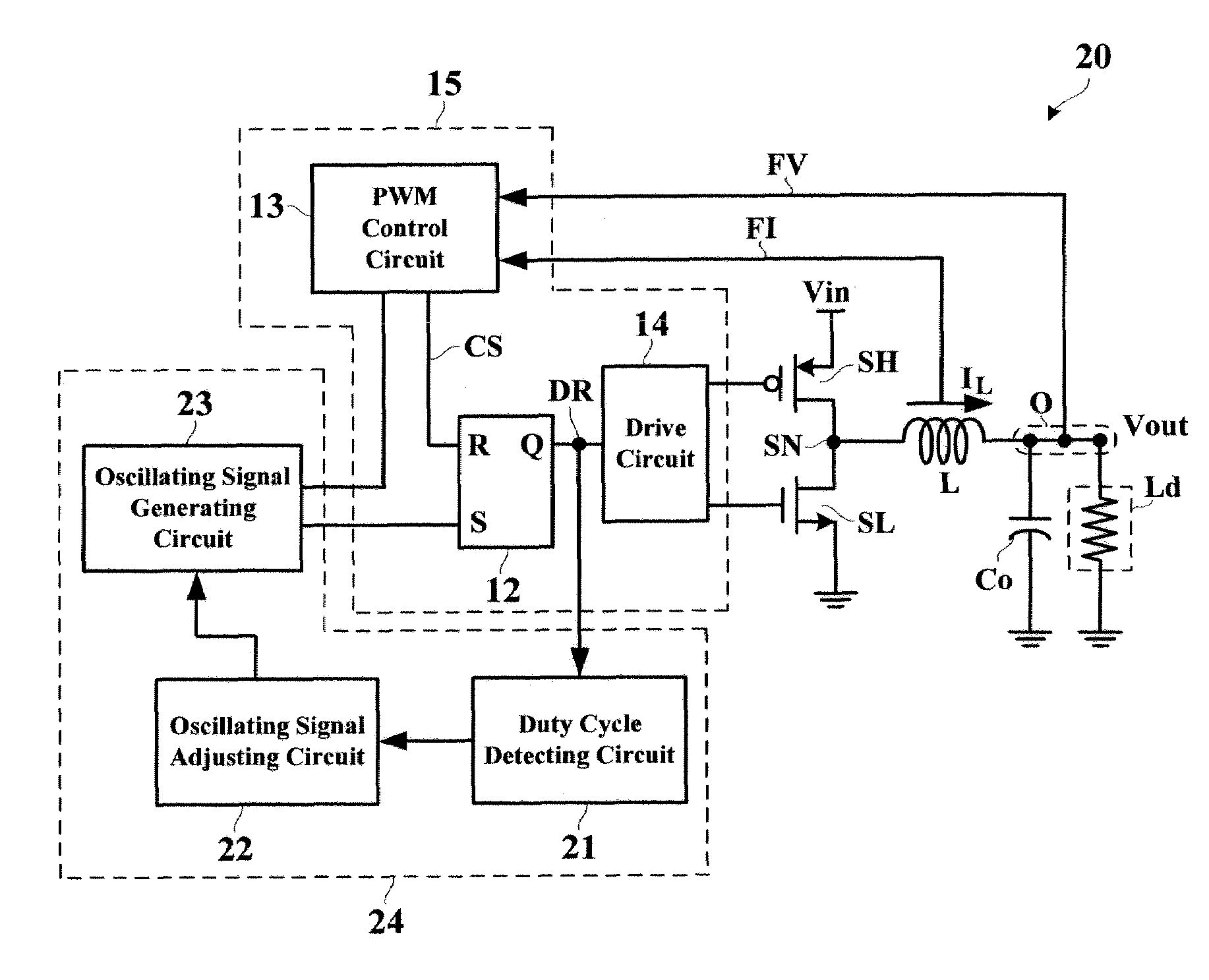
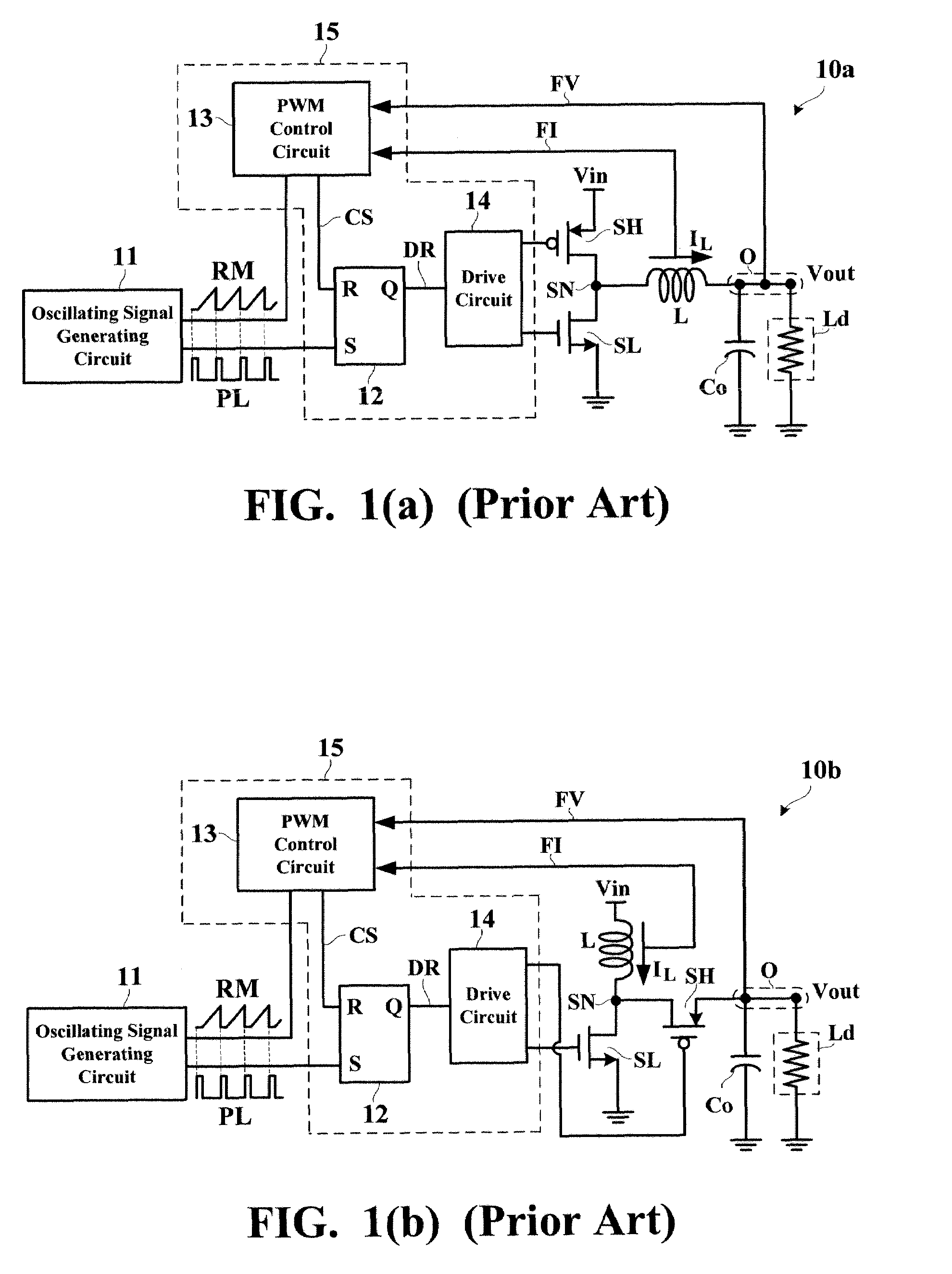
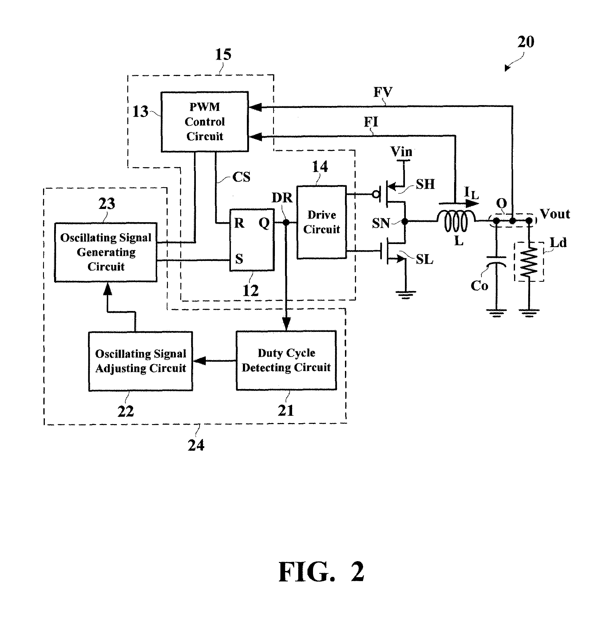
[0025]FIG. 2 is a circuit diagram showing a switching voltage regulator 20 according to a first embodiment of the present invention. The switching voltage regulator 20 belongs to the step-down type, i.e., converting the higher input voltage Vin into the lower output voltage Vout. The switching voltage regulator 20 has a switch control system 15 and an oscillating signal generating system 24. The switch control system 15 is constituted by a latch 12, a PWM control circuit 13, and a drive circuit 14. The oscillating signal generating system 24 is constituted by a duty cycle detecting circuit 21, an oscillating signal adjusting circuit 22, and an oscillating signal generating circuit 23.

[0026]More specifically, the duty cycle detecting circuit 21 detects the duty cycle Da of the drive signal DR. When the input voltage Vin becomes closer to the output voltage Vou...


PUM


Abstract

A switching voltage regulator has a first switch, a second switch, and an inductor, which are coupled together to a switch node. A switch control system applies a drive signal for controlling the first and the second switches. A duty cycle detecting circuit detects a duty cycle of the drive signal. When the duty cycle is larger than a predetermined threshold, the duty cycle detecting circuit generates an over-threshold signal. When the duty cycle is smaller than the predetermined threshold, the duty cycle detecting circuit generates an under-threshold signal. In response to the over-threshold signal and the under-threshold signal, an oscillating signal adjusting circuit generates an adjusting current. An oscillating signal generating circuit generates and applies an oscillating signal to the switch control system. The oscillating signal has a period adjusted by the adjusting current.

Description

BACKGROUND OF THE INVENTION[0001]1. Field of the Invention[0002]The present invention relates to a switching voltage regulator and, more particularly, to a switching voltage regulator with an improved range of input voltage.[0003]2. Description of the Related Art[0004]FIG. 1(a) is a circuit diagram showing a conventional switching voltage regulator 10a. The switching voltage regulator 10a converts an input voltage Vin into an output voltage Vout for being supplied to a load Ld. A high-side switch SH is coupled between the input voltage Vin and a switch node SN while a low-side switch SL is coupled between the switch node SN and a ground potential. As to the example of FIG. 1(a), the high-side switch SH is implemented by a PMOS transistor while the low-side switch SL is implemented by an NMOS transistor. An inductor L is coupled between the switch node SN and an output terminal O. An output capacitor Co is coupled to the output terminal O for filtering the output voltage Vout.[0005]T...

Claims


Application Information

Patent Timeline
04 Mar 2008
Publication
US7339360B2
IPC
G05F1/40; G05F1/56
CPC
H02M3/1563
Inventors
CHEN, TIEN-TZU; CHEN, LI-CHENG