Shift register circuit

a technology of shift register and shift register, applied in the field of shift register, can solve problems such as incorrect lcd output, and achieve the effect of reducing the layout area of the circui

Active Publication Date: 2008-03-11
AU OPTRONICS CORP
View PDF3 Cites 6 Cited by
  • Summary
  • Abstract
  • Description
  • Claims
  • Application Information

AI Technical Summary

Benefits of technology

[0008]The invention provides a shift register capable of reducing the circuit layout area.

Problems solved by technology

Take the output signal of the (N−1)th stage shift register for example, the discharge time thereof is about 25 μs and when the output signal of the Nth stage shift register charges, the output signal of the (N−1)th stage shift register does not discharge completely, thus, an overlap occurs, and this causes the incorrect LCD output.

Method used


Image

  • Shift register circuit
  • Shift register circuit
  • Shift register circuit

Examples


Embodiment Construction

[0021]The following description is of the best-contemplated mode of carrying out the invention. This description is made for the purpose of illustrating the general principles of the invention and should not be taken in a limiting sense. The scope of the invention is best determined by reference to the appended claims.

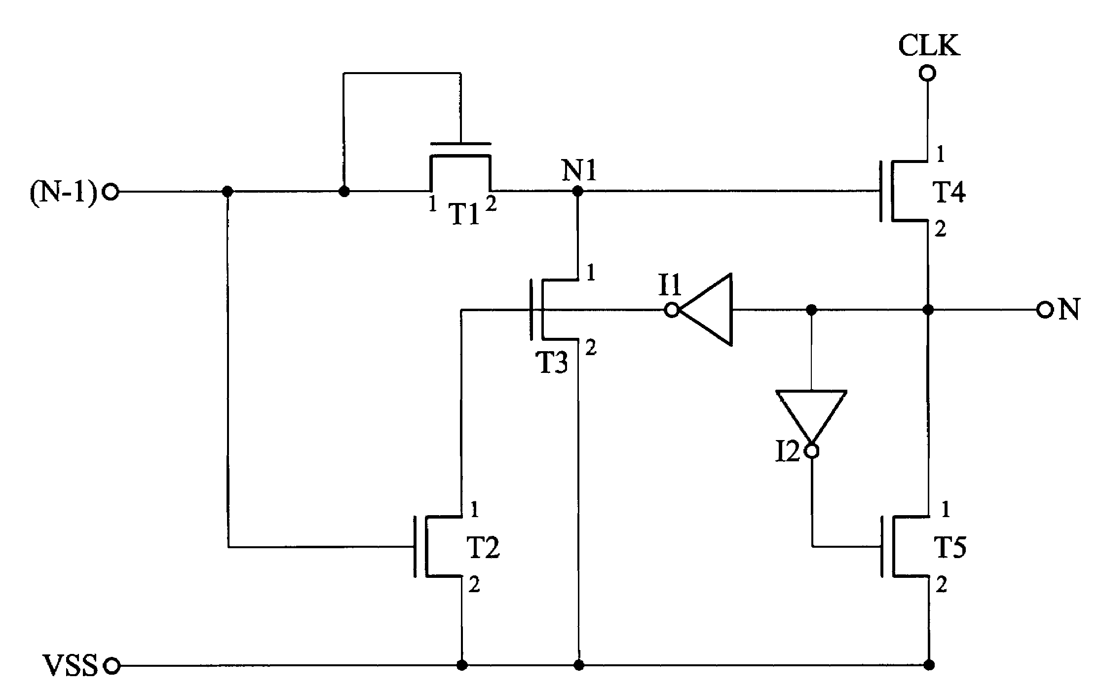
[0022]FIG. 3 is a circuit diagram of a shift register of an embodiment of the invention. The gate and first source / drain of transistor T1 is coupled to an output signal N−1 of a pre-stage, (N−1)th stage, shift register and the transistor T1 turns on when the output signal of the pre-stage shift register is at high voltage level. The second source / drain of transistor T1 is coupled to the gate of transistor T4. The first source / drain of transistor T4 is coupled to a clock signal CLK, and the second source / drain of transistor T4 is coupled to an output signal N of the Nth stage shift register. The gate of transistor T2 is coupled to the first source / drain of transistor T1...


PUM


Abstract

A shift register without a feedback signal of a post-stage shift register utilizing a latch mechanism and a clock signal to control the voltage of an output of the shift register is provided. The shift register reduces the transistor size and the circuit layout area. The shift register also improves the issue the overlapping between two adjacent shift registers to reduce the after-image of a liquid crystal display.

Description

BACKGROUND OF THE INVENTION[0001]1. Field of the Invention[0002]The invention relates to a shift register and more particularly to a shift register without a feedback signal from an output signal of a post-stage shift register.[0003]2. Description of the Related Art[0004]Liquid crystal displays (LCD) have become the major product of displays, and minimizing the size and the weight of the LCDs, to dispose the driving circuit on the substrate of the LCD has become a major technology focus. Take the TFT LCD for example, since the amorphous Si process is the main technology, the low electron mobility of amorphous Si limits the size of the element formed by the amorphous Si process, such as a thin film transistor (TFT). If the transistor formed by the amorphous Si process wants to receive a larger current, the width of the channel of the transistor increases, thus, the layout area increases.[0005]FIG. 1 is a circuit diagram of a conventional amorphous Si shift register. To ensure that th...

Claims


Application Information

Patent Timeline
Patent Type & Authority Patents(United States)
IPC IPC(8): G11C19/00
CPCG11C19/00G11C19/28
Inventor WEI, CHUN-CHINGWU, YANG-ENLIN, WEI-CHENG
Owner AU OPTRONICS CORP
Why Eureka
Try Eureka