Stamping system for manufacturing high tolerance parts

a stamping system and high tolerance technology, applied in forging presses, shaping tools, instruments, etc., can solve the problems of large number of components required in the deployment of fiber for these types of applications, sensitive to the cost of e-o-e terminal conversion devices and supporting circuitry, and the cost of both active and passive fiber components, so as to achieve tight tolerances and reduce the number of moving components

Active Publication Date: 2008-03-18
SENKO ADVANCED COMPONENTS
View PDF39 Cites 87 Cited by
  • Summary
  • Abstract
  • Description
  • Claims
  • Application Information

AI Technical Summary

Benefits of technology

[0011]In one aspect of the present invention, the system is designed to minimize the number of moving components involved in the support structure in guiding the punch to the die. In one embodiment, the stamping station includes no moving component in the support structure in guiding the punch to the die. The stamping station includes a stationary punch holder structure having a shaft sized and shaped to receive the punch with tight tolerances. The punch is guided to the die by sliding through the shaft.
[0012]In another aspect of the present invention, the system includes a locating sub-plate having indexing features for precisely aligning the progression of stamping stations relative to each other. The locating sub-plate and its indexing features have exacting tolerances and sub-micron surface finishes.

Problems solved by technology

The number of components required in the deployment of fiber for these types of applications is large.
In these short systems, fiber optics “prove-in” is very sensitive to the cost of E-O-E terminal conversion devices and supporting circuitry, as well as any passive and active optoelectronic devices and equipment linked between terminal ends.
A significant element of the cost of both active and passive fiber components and connectorized cable is the fiber connector itself.
Current connectors have not changed in basic design for more than 20 years, and it is generally accepted that they cost too much and are too difficult to assemble.
However, heretofore, stamping processes have not been effective in producing parts with acceptable tolerances for optoelectronic components.
In fact, there is no acceptable high-speed commercial production process that produces optoelectronic components with acceptable tolerances.
However, Balliet does not provide an enabling disclosure of such stamping process, let alone an enabling disclosure of a stamping process for producing parts within 1000 nm.

Method used


Image

  • Stamping system for manufacturing high tolerance parts
  • Stamping system for manufacturing high tolerance parts
  • Stamping system for manufacturing high tolerance parts

Examples


first embodiment

Stamping Station—First Embodiment

[0058]FIG. 3a is a perspective view of a stamping station 400 in accordance with one embodiment of the present invention. FIG. 3b is a sectional view of the stamping station taken along line 3b-3b shown in FIG. 3a. The stamping station 400 includes structure for supporting the die set assembly and for directly guiding the punch to the die. The stamping station 400 includes a stationary punch holder plate 410, for supporting a punch 420, and a die holder plate 440, for supporting a die 450. The punch holder plate 410 functions to align and directly guide the punch 420 to the die 450. The punch holder plate 410 has a shaft 430 sized and shaped to slidably receive the punch 420 and to guide the punch 420 to the die 450. The shaft 430 allows the punch 420 to translate and penetrate through the punch holder plate 410, in slidable contact with the shaft 430. The shaft 430 aligns the punch 420 with the die 450, guiding the punch 420 to a work piece 455 and ...

second embodiment

Stamping Station—Second Embodiment

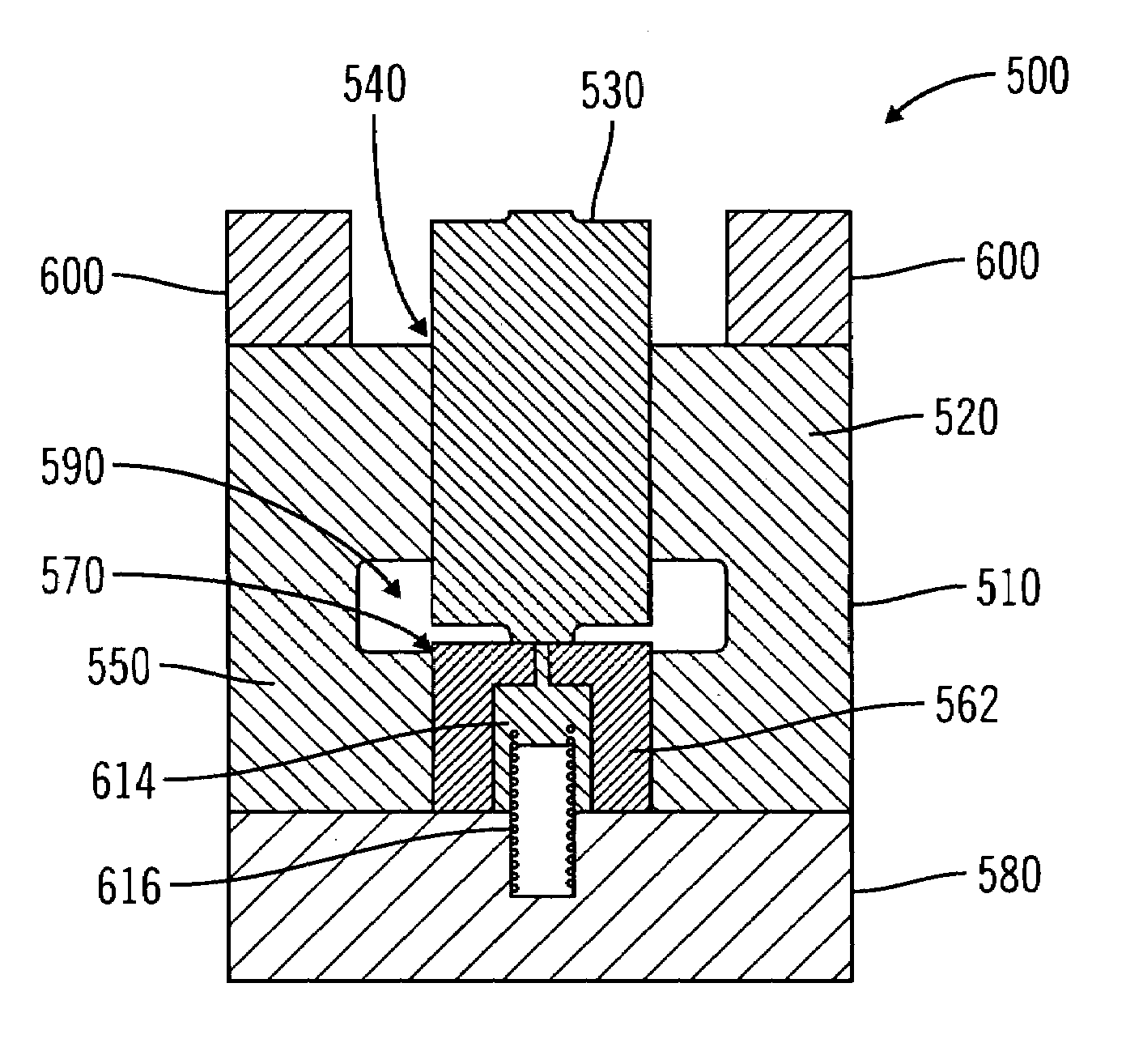
[0063]FIG. 4 is a perspective view of a stamping station 500 in accordance with another embodiment of the present invention. FIG. 5 is an assembly view of the stamping station 500 shown in FIG. 4. FIGS. 6a and 6b are sectional views of the stamping station 500 shown in FIG. 4, taken along lines 6a-6a and 6b-6b respectively. The stamping station 500 includes a stationary, monolithic die set assembly holder structure 510 for supporting the die set assembly. The die set holder 510 includes a punch holder section 520 for supporting and guiding a punch 530. The punch holder section 520 has a shaft 540 sized and shaped to slidably receive and support the punch 530. The shaft 540 is shown in FIG. 6. The shaft 540 allows the punch 530 to translate and penetrate through the die set holder 510. The punch 530 slides in contact within the shaft 540. The shaft 540 facilitates aligning the punch 530 relative to the die, guiding the punch 530 to a work piece 595 (...

third embodiment

Stamping Station—Third Embodiment

[0067]FIG. 8a is a schematic view of a stamping station 800 in accordance with another embodiment of the present invention. The stamping station 800 includes a die holder plate 850, for supporting a die 840, and a shaft 810 for supporting and guiding a punch 860 to the die 840. The shaft 810 is sized and shaped to slidably receive and support the punch 860, allowing the punch 860 to translate longitudinally through the shaft 810 towards and away from the die 840. The shaft 810 facilitates alignment of the punch 860 with the die 840, guiding the punch 860 to the die 840. Adjustable mechanical stoppers 880 are located in the stroke path of the punch 860 for limiting the translation of the punch 860 towards the die 840. The punch 860 is provided with a catch 830 which can engage the stoppers 880 to limit further translation of the punch 860 towards the die 840. A spacer 895 is provided for adjusting the position of the mechanical stoppers 880 relative t...


PUM

PropertyMeasurementUnit
surface roughnessaaaaaaaaaa
diameteraaaaaaaaaa

Abstract

A system and process for stamping parts having tolerances below 1000 nanometers. The inventive system and process is particularly suited for producing optoelectronic parts. The system includes a stamping press and one or a progression of stamping stations for supporting a punch and die. The stamping stations are designed to maintain substantial alignment of the punch and die with minimal moving components. The stamping station includes a shaft for rigidly guiding the punch to the die. The stamping press is capable of providing the punch with the necessary force to perform the stamping operations. The system includes an interface system for interfacing the force of the press with the punch, while simultaneously structurally decoupling the press from the punch. The system also includes a locating sub-plate, for locating the stamping station in alignment relative to each other, and means for in-line machine stock material before entry into the stamping stations.

Description

BACKGROUND OF THE INVENTION[0001]1. Field of the Invention[0002]The present invention relates to stamping system and processes, and more particularly stamping processes for manufacturing parts with high tolerances for various applications, such as optical fiber connection.[0003]2. Description of Related Art[0004]Precision parts are required in many applications, such as optical fiber based communication. Optical fiber based communication channels are the system of choice in many defense and commercial applications because of their high performance and small size. Particularly, fiber optics have “proved-in” in long distance applications, such as city-to-city and continent-to-continent communication spans, because of the lower cost of electrical-to-optical-to-electrical (E-O-E) conversion components, fiber amplifiers, and fiber cables relative to pure electrical systems using coaxial copper cable that do not requiring E-O-E. These long haul fiber systems can have hundreds of kilometer...

Claims


Application Information

Patent Timeline
Patent Type & Authority Patents(United States)
IPC IPC(8): B21D28/26B21J13/04B26D5/08G02B6/36B21D22/02B21D28/02B21D37/12B26F1/40G02B6/38
CPCB21D28/02B21D37/12B26F1/40G02B6/3885G02B6/3834G02B6/3839G02B6/3855G02B6/3862G02B6/3833G02B6/3636G02B6/3652G02B6/3877Y10T83/4635Y10T83/8855Y10T83/9423Y10T83/9476G02B6/00G02B6/36
Inventor BARNOSKI, MICHAEL KCOHEN, DAVIDHARRIS, DANKANG, SANGKYUNLEVI, ANTHONYPINILLA, MIGUELPRINZ, FRITZTARASYUK, ALEX
Owner SENKO ADVANCED COMPONENTS
Why Eureka
Try Eureka