

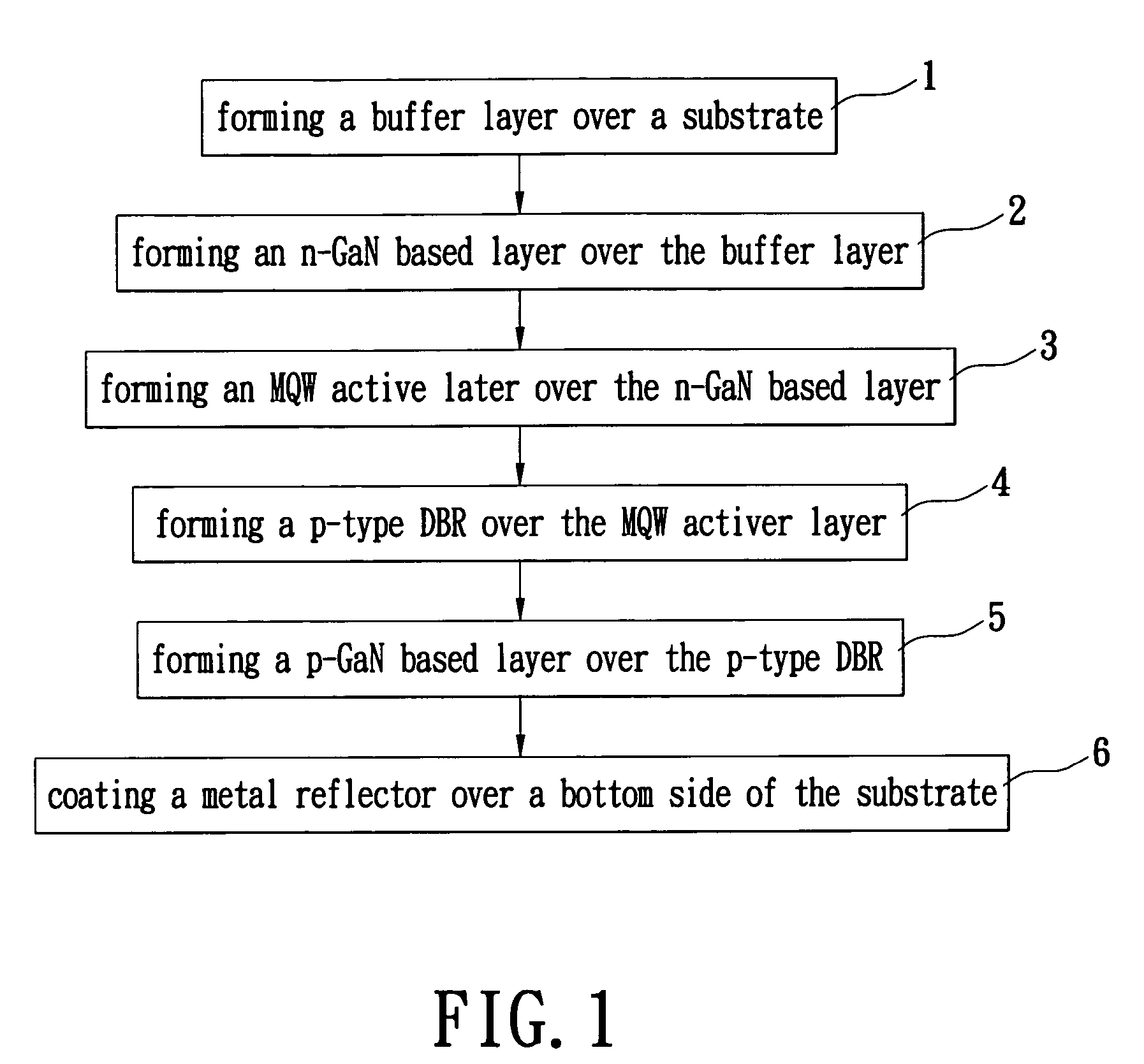
Gallium nitride based light-emitting device
a technology of light-emitting devices and gallium nitride, which is applied in the manufacturing of semiconductor/solid-state devices, semiconductor devices, electrical devices, etc., can solve the problems of insufficient brightness of current leds, and achieve the effects of reducing cost, high luminous efficiency, and simplifying manufacturing process
- Summary
- Abstract
- Description
- Claims
- Application Information
AI Technical Summary
Benefits of technology
Problems solved by technology
Method used
Image

Examples
second embodiment
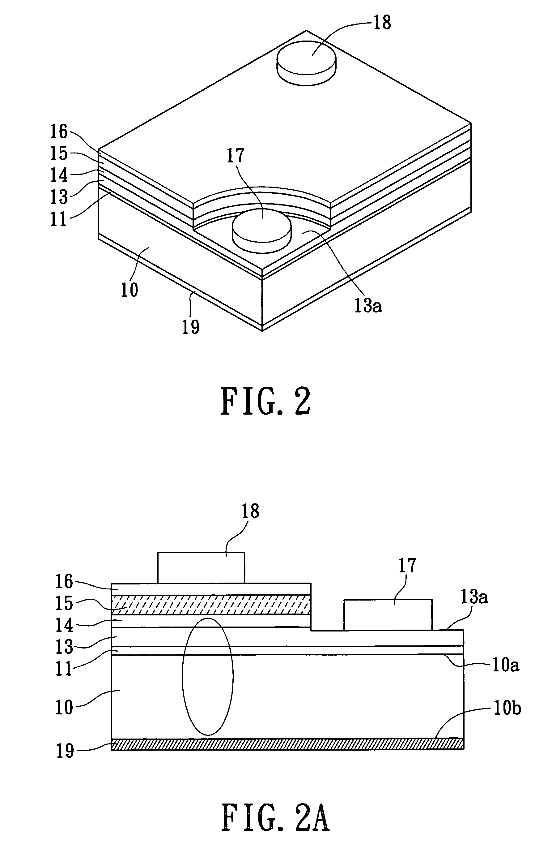
[0042]Now the description will be made to a second embodiment according to the present application, and please refer directly to FIG. 4. The second method embodiment is the same as the preferred embodiment except to the step, Step 6′. Step 6′: coating a transparent contact layer (TCL) with a suitable thickness over the contact layer, p-GaN based layer, succeeding to Step 5. In terms of material used, the TCL may be made of Ni / Au and other suitable transparent (for the generated light from the light-emitting structure, such as a light with a wavelength of 380-600 nm) and conductive material and may be an n-TCL (n-doped) or a p-TCL (p-doped). In fact the TCL may be a doped metal, such as doped ZnO, which may be referenced to U.S. Pat. No. 6,992,331, published on Jan. 31, 2006, which is assigned to the same assignee as the present invention.
[0043]The second device embodiment according to the present invention is manufactured by the second method embodiment and provided schematically as...
fourth embodiment
[0048]The device of the fourth embodiment according to the present invention, FIGS. 9 and 9A, includes a substrate 30, an n-DBR 32, an n-GaN layer 34, an MQW active layer 35, a p-DBR 36, a contact layer 37, an n-type metal electrode 38 and a p-type electrode 39.
[0049]As compared to the former three embodiments, the fourth device embodiment is different in the resonant cavity, which is formed between the n-DBR 34 and the p-DBR 36 (the metal reflector 19 and the p-DBR 15 in the afro-mentioned embodiments), and the substrate 30 is not included in the resonant path. In this case, the substrate 30 may be transparent or not transparent, such as silicon, which is contrary to the transparent substrate 10 in the above embodiments.
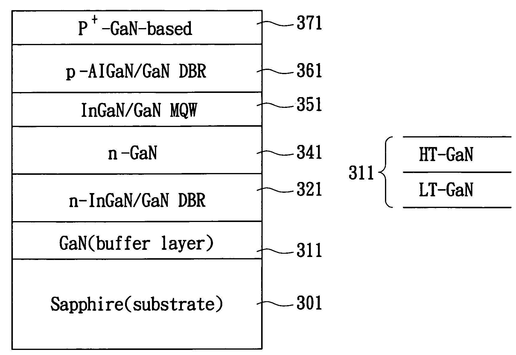
[0050]Referring to FIGS. 10 and 10A, a particular example of FIGS. 9 and 9A is shown there. In the example, the first and second layer 311 is an LT-GaN / HT-GaN buffer layer, the third layer 321 is an n-AlGaN / GaN DBR, the fourth layer 341 is an n-GaN semiconductor lay...
PUM
 Abstract
Description
Claims
Application Information