Programmable logic devices with two-phase latch circuitry

a latch circuit and logic device technology, applied in the field of programmable logic devices, can solve the problems of limiting the speed at which the pld can be made to operate (i.e., clocked), not being able to decrease the period of the clock, and undesiredly increasing the latency of the signal(s) being propagated, so as to achieve the effect of “borrowing

Inactive Publication Date: 2008-03-18
ALTERA CORP
View PDF6 Cites 33 Cited by
  • Summary
  • Abstract
  • Description
  • Claims
  • Application Information

AI Technical Summary

Benefits of technology

[0003]To address problems like the foregoing, a PLD is provided with level-sensitive latches in lieu of or as an alternative to single-phase, edge-triggered data signal storage elements. Each such level-sensitive latch is preferably selectively clockable with either of the two phases (true and complement) of a clock signal. A latch that is clocked by a first of the two phases (e.g., the true or high phase) may be referred to as a high-phase latch. A latch that is clocked by a second of the two phases (e.g., the complement or low phase) may be referred to as a low-phase latch. The paths through which data signals propagate are interspersed with alternating high- and low-phase latches. For example, a path that in a prior art design would have extended from a first single-phase, edge-triggered flip-flop through a second single-phase, edge-triggered flip-flop to a third single-phase, edge-triggered flip-flop may be implemented in accordance with this invention by a path extending from a first high-phase latch (taking the place of the first flip-flop), thr

Problems solved by technology

This limits the speed at which the PLD can be made to operate (i.e., clocked) to the maximum signal propagation delay from one register to another register on the device.
Even if the propagation delay between other regist

Method used


Image

  • Programmable logic devices with two-phase latch circuitry
  • Programmable logic devices with two-phase latch circuitry
  • Programmable logic devices with two-phase latch circuitry

Examples


Embodiment Construction

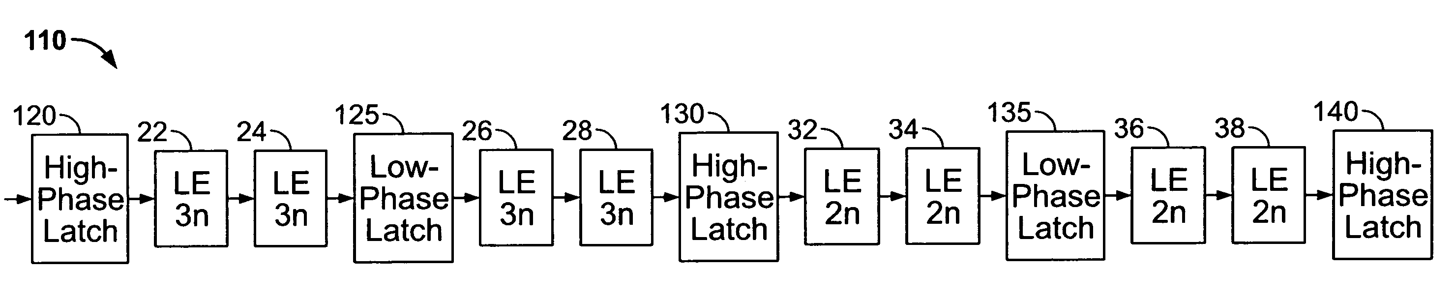
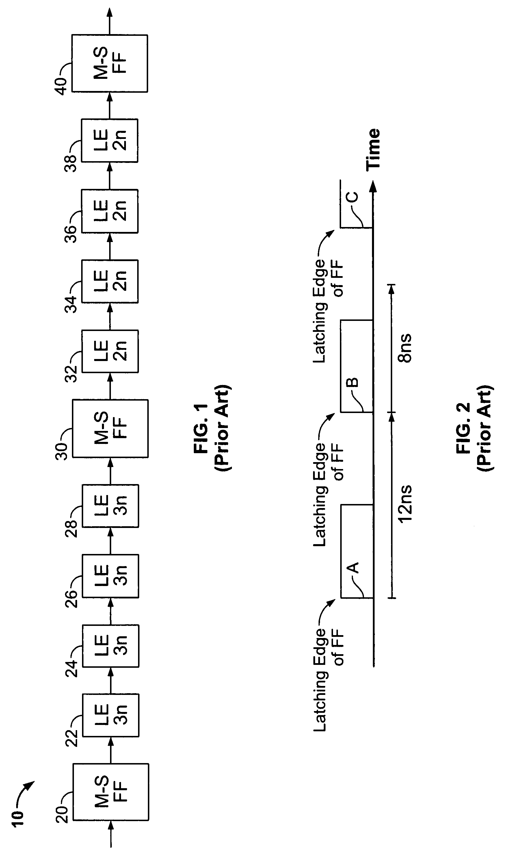
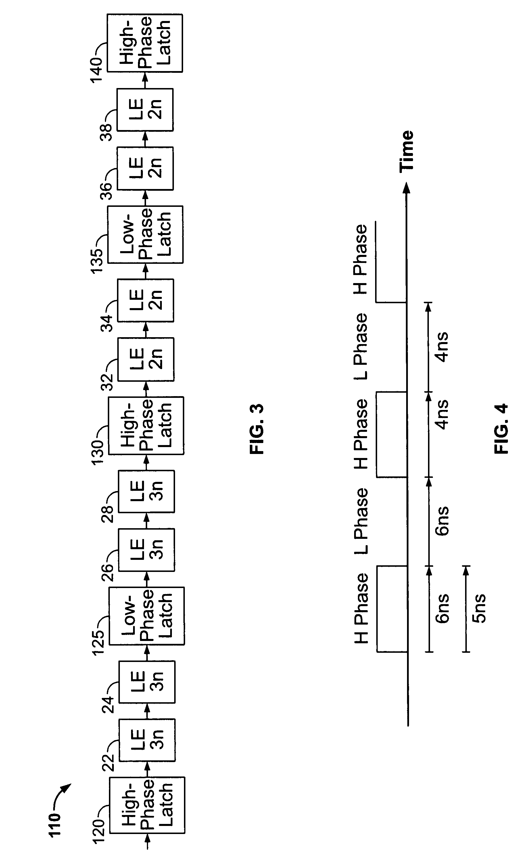
[0024]FIG. 1 shows some representative prior art PLD circuitry 10 to illustrate issues addressed by this invention. Circuitry 10 includes a first master-slave (“M-S”) flip-flop (“FF”) 20, from which data propagates successively through logic elements (“LEs”) 22, 24, 26, and 28 to second master-slave flip-flop 30. From flip-flop 30 data propagates successively through logic elements 32, 34, 36, and 38 to third master-slave flip-flop 40. Each of logic elements 22-28 is characterized by a propagation delay of 3 nanoseconds (“n” or “ns”). Each of logic elements 32-38 is characterized by a propagation delay of 2 nanoseconds. Accordingly, the register to register delay from FF 20 to FF 30 is 12 ns. The register to register delay from FF 30 to FF 40 is 8 ns. (Although FIG. 1 shows only LEs, it will be understood that a PLD may also include other types of circuit modules such as memory blocks, digital signal processing (“DSP”) blocks, etc., and that any one or more of the LEs in FIG. 1 or i...


PUM


Abstract

Programmable logic circuitry includes level-sensitive latches as at least some of the data storage elements. At least some of the latches are enabled by one phase of a clock signal, and at least some others of the latches are enabled by the other phase of the clock signal. Accordingly, these latches collectively have two-phase operation. These two-phase latches may replace at least some single-phase, edge-triggered flip-flops in a user's logic design, and may thereby increase the speed at which the user's logic can be operated. Methods for converting a single-phase, edge-triggered flip-flop design to a logically equivalent design using at least some two-phase latches are disclosed.

Description

BACKGROUND OF THE INVENTION[0001]This invention relates to programmable logic devices (“PLDs”), and more particularly to PLDs that include or that can include two-phase latches.[0002]PLDs typically use single-phase, edge-triggered data storage circuitry (e.g., flip-flops) to register data signals propagating through the processing or logic circuitry of the PLD. This limits the speed at which the PLD can be made to operate (i.e., clocked) to the maximum signal propagation delay from one register to another register on the device. For example, if the maximum propagation delay between two single-phase, edge-triggered registers is 12 nanoseconds (“ns”), the period of the clock cannot be less than 12 ns. Even if the propagation delay between other registers is less than 12 ns, the slowest path controls, and it is not possible to decrease the period of the clock. Introducing another register in the path between two registers having a long inter-register propagation delay may decrease the ...

Claims


Application Information

Patent Timeline
IPC IPC(8): G06F17/50
CPCG06F17/5054G06F17/5059G06F30/34G06F30/35
Inventor LEE, ANDY L
Owner ALTERA CORP
Why Eureka
Try Eureka