Multi-chip module

a multi-chip module and chip technology, applied in the direction of semiconductor devices, electrical equipment, semiconductor/solid-state device details, etc., can solve the problems of large signal delay caused by wiring, restricted improvement in speed and miniaturization of resulting devices, and difficulty in shortening the their wiring distance, so as to reduce the mounting area, shorten the wiring distance between the respective chips, and improve the characteristics of the semiconductor device

Active Publication Date: 2008-04-01
RENESAS ELECTRONICS CORP
View PDF5 Cites 16 Cited by
  • Summary
  • Abstract
  • Description
  • Claims
  • Application Information

AI Technical Summary

Benefits of technology

[0010]On the other hand, in the multi-chip module (Multi Chip Module) technology, a plurality of semiconductor chips in the form of a remarkably small, so-called bear chip are employed and made into a semiconductor device in the form of one package, and as a result, the wiring distance between the respective chips can be shortened and the characteristics of the semiconductor device can be improved. The semiconductor device can be miniaturized by putting the plurality of chips into one package, and the semiconductor device can be miniaturized by decreasing the mounting area. In the Patent References 1 to 3, attention is not paid to improvement in the function and further miniaturization of the device as a whole which are the features of MCM (multi-chip module), but rather the respective chips are just made into the stack structure.

Problems solved by technology

This is because when not a plurality of semiconductor chips but a plurality of semiconductor devices obtained by respectively packaging semiconductor chips by a usual packaging technique such as QFP (Quad Flat Package), CSP (Chip Size Package or Chip Scale Package), or BGA (Ball Grid Array) are employed and the plurality of semiconductor devices are mounted on a mounting board such as a printed circuit board, it becomes difficult to shorten the distance between the semiconductor chips and their wiring distance, and as a result, a signal delay caused by wiring becomes large and improvement in the speed and miniaturization of the resulting device are restricted.

Method used


Image

  • Multi-chip module
  • Multi-chip module
  • Multi-chip module

Examples


Embodiment Construction

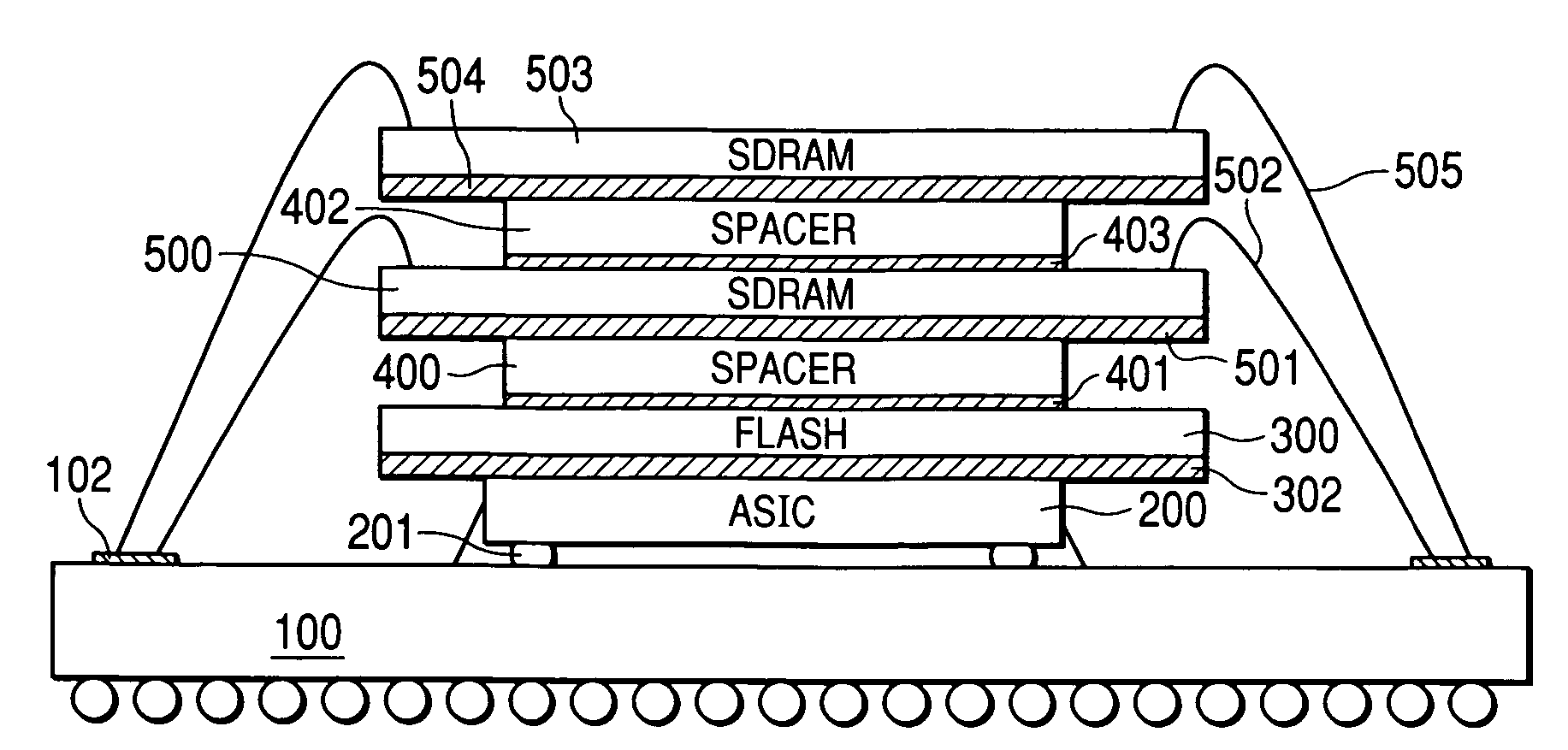
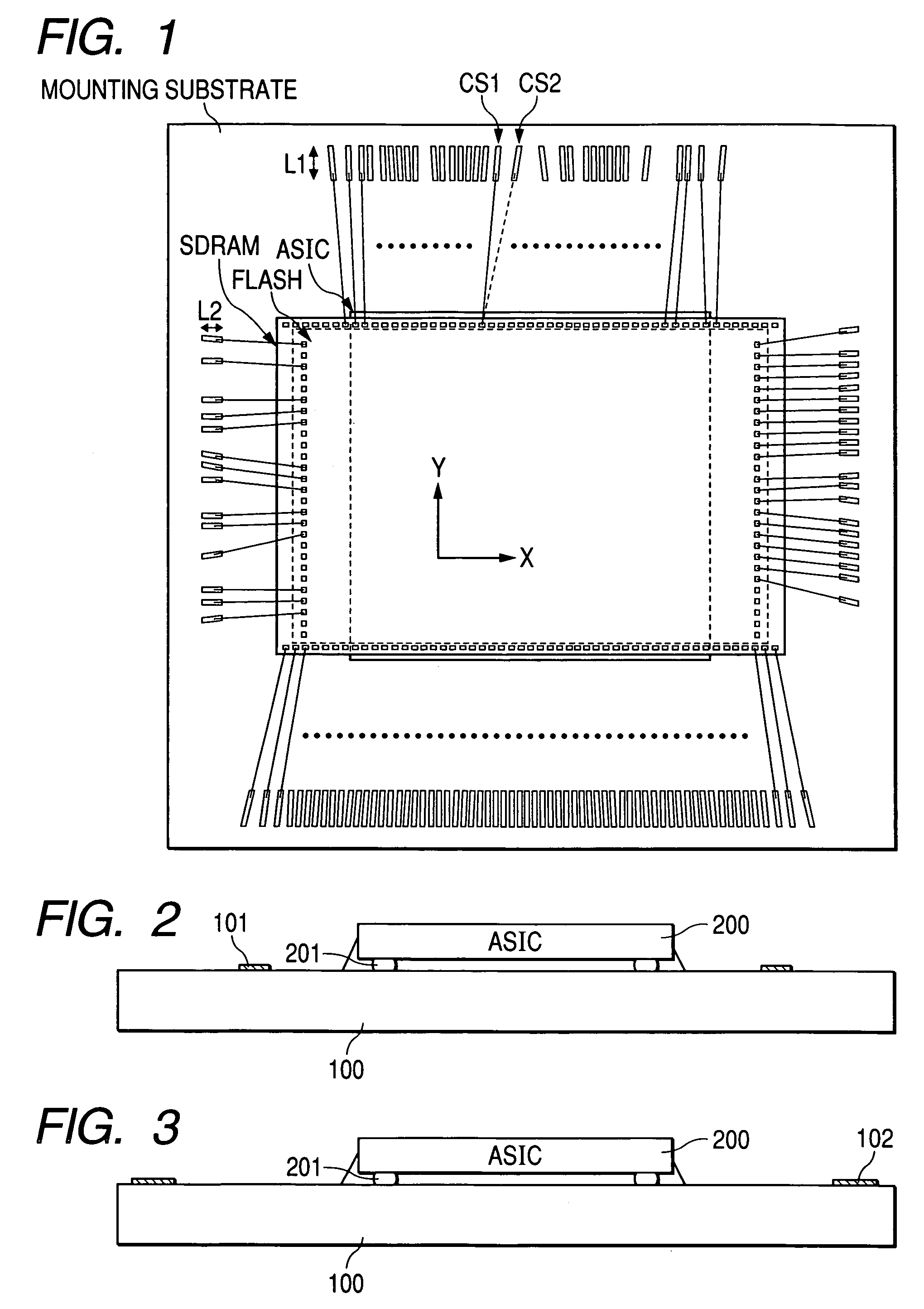
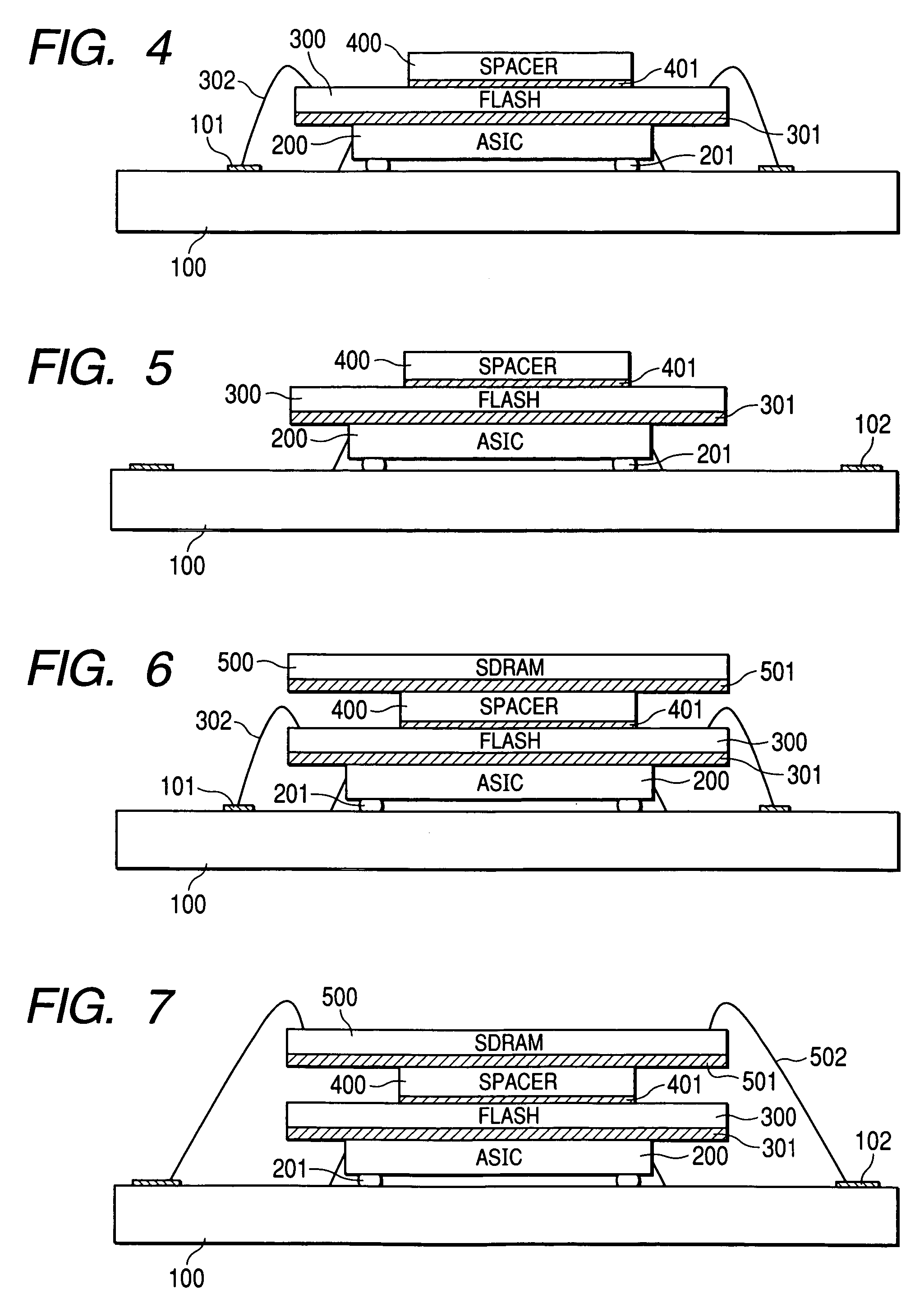
[0027]An outline plan view of one example of MCM (SiP) concerning this invention is shown in FIG. 1. On a mounting substrate surface, an application specific IC (henceforth ASIC) which has a one-chip microcomputer function containing CPU (central processing unit) is surface-mounted. On the surface of this ASIC, a nonvolatile memory (henceforth FLASH) is mounted back-to-back to the ASIC, and a synchronous DRAM (henceforth SDRAM) is mounted via a spacer on it. The above FLASH is a so-called AND type although not restricted in particular, and does not have any independent address terminal although not restricted in particular. An address signal is serially inputted in a time sharing manner using a data terminal. For this reason, bonding pads are arranged along the FLASH chip perimeter at both sides in the Y direction in this drawing, electrodes are arranged on a mounting substrate corresponding to these bonding pads, and connected to these bonding pads through wires.

[0028]In the SDRAM,...


PUM


Abstract

A multi-chip module is provided which allows memory space extension to improve function and performance. A first semiconductor chip is mounted on a mounting substrate, and a first semiconductor memory chip is mounted over the first semiconductor chip. A second semiconductor memory chip having the same circuitry and the same memory capacity as the first semiconductor memory chip is mounted on a spacer formed on the first memory chip in the same direction as the first semiconductor memory chip. An electrode is independently formed corresponding to a bonding pad to which a selective signal of the first semiconductor memory chip and the second semiconductor memory chip is supplied. A plurality of electrodes are formed in common corresponding to a plurality of bonding pads to which the same signal is respectively supplied except for the selective signal.

Description

CROSS-REFERENCE TO RELATED APPLICATIONS [0001]The present application claims priority from Japanese patent application No. 2004-349016 filed on Dec. 1, 2004, the content of which is hereby incorporated by reference into this application.[0002]1. Field of the Invention[0003]This invention relates to a multi-chip module (MCM), and for example, relates to an effective technology in the application to a multi-chip module in which a plurality of semiconductor chips with some functions different from one another are integrated as substantially one semiconductor integrated circuit device by mounting them on one mounting substrate.[0004]2. Description of the Background Art[0005]In the so-called multi-chip module technology, a plurality of semiconductor chips are mounted on a mounting substrate which has a plurality of internal wirings and a plurality of external terminals, and these semiconductor chips and the mounting substrate are integrated with each other as a device. Japanese Unexamine...

Claims


Application Information

Patent Timeline
Patent Type & Authority Patents(United States)
IPC IPC(8): H01L23/40
CPCH01L23/18H01L23/3128H01L25/0657H01L25/18H01L21/563H01L2224/16225H01L2224/32145H01L2224/48091H01L2224/48227H01L2224/49171H01L2224/73203H01L2224/73204H01L2224/73253H01L2224/73265H01L2225/0651H01L2225/06517H01L2225/06555H01L2924/01079H01L2924/1433H01L2924/15311H01L2924/30107H01L2924/00014H01L24/48H01L24/49H01L2924/01021H01L2924/00H01L2224/32225H01L2924/00012H01L24/73H01L2924/14H01L2924/181H01L2224/05554H01L2924/10161H01L2224/45099H01L2224/45015H01L2924/207
Inventor KURODA, HIROSHITETSUKA, MAKOTO
Owner RENESAS ELECTRONICS CORP
Why Eureka
Try Eureka