Electroluminescent display panel and electronic device

a technology of electronic devices and display panels, applied in static indicating devices, cathode-ray tube indicators, instruments, etc., can solve the problems that the film process may not allow the adoption of p-channel thin film transistors, and achieve the effect of reducing the number of times the power supply line three-dimensionally crosses the wiring of the other driving sections, reducing the load on the power supply line driving sections, and high resistance valu

Inactive Publication Date: 2009-05-14
SONY CORP
View PDF12 Cites 21 Cited by
  • Summary
  • Abstract
  • Description
  • Claims
  • Application Information

AI Technical Summary

Benefits of technology

[0031]In addition, by arranging the power supply line driving sections on the inside of the writing control line driving sections, the number of times that the power supply line three-dimensionally crosses wiring of the other driving sections can be reduced. Normally, wiring having a relatively high resistance value is used as wiring at intersecting parts because of a process. Decreasing three-dimensional intersecting parts is therefore effective in reducing a load on the power supply line driving sections.
[0032]It is thereby possible to decrease a voltage drop in the power supply line at a time of white display. This means a reduction in difference between voltage drops at a time of white display and at a time of black display. Hence, uniform image quality free from not only crosstalk but also shading can be obtained.

Problems solved by technology

That is, the present thin film process may not allow the adoption of the p-channel type thin film transistor.

Method used


Image

  • Electroluminescent display panel and electronic device
  • Electroluminescent display panel and electronic device
  • Electroluminescent display panel and electronic device

Examples


first embodiment

(B) First Embodiment

(B-1) System Configuration

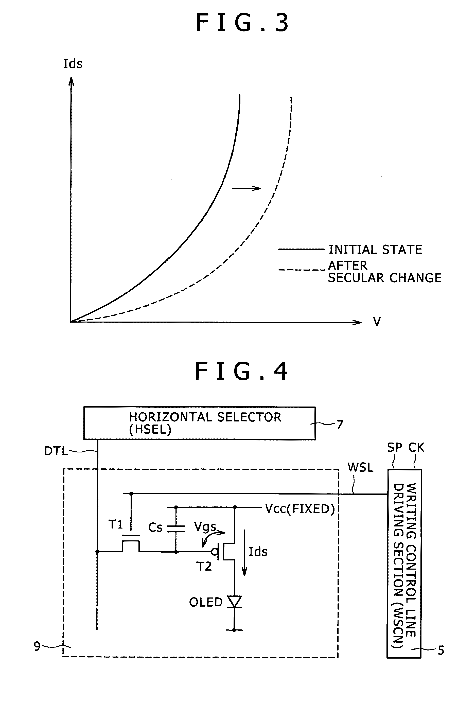
[0083]An example of system configuration of the organic EL panel 11 that prevents variations in characteristics of a driving transistor T2 and requires only a small number of elements forming a pixel circuit will be shown in the following. Incidentally, the present embodiment assumes an organic EL panel having a large screen size.

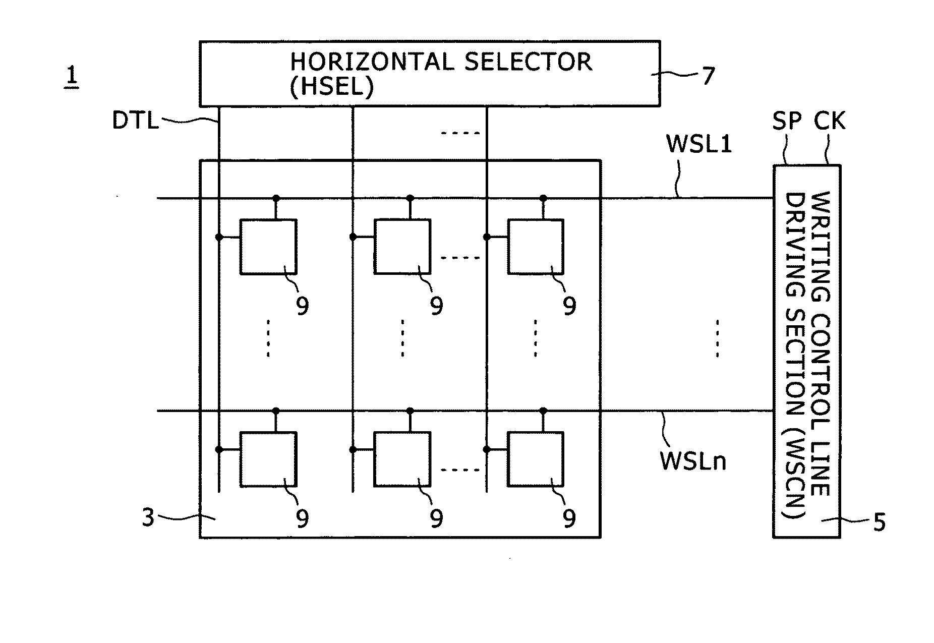
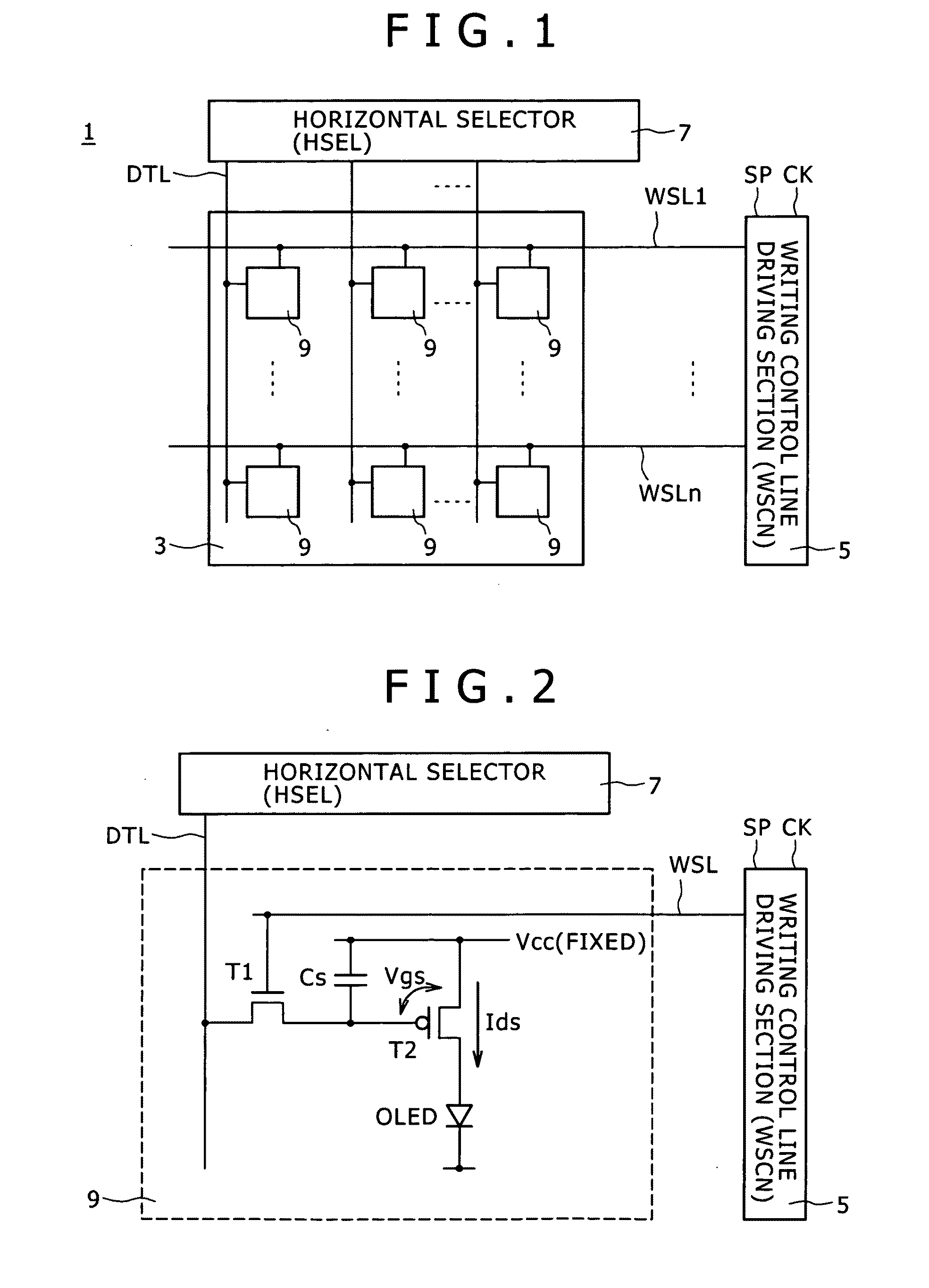
[0084]FIG. 6 shows an example of system configuration of the organic EL panel 11. The organic EL panel 11 shown in FIG. 6 includes a pixel array section 21, writing control line driving sections 23 and power supply line driving sections 25 as driving circuits for the pixel array section 21, a horizontal selector 27, and a timing generator 29.

[0085]The pixel array section 21 has a matrix structure in which a sub-pixel is disposed at each intersecting position of a signal line DTL and a writing control line WSL. Incidentally, a sub-pixel is a minimum unit of a pixel structure forming one pixel. For example, one pi...

second embodiment

(C) Second Embodiment

(C-1) System Configuration

[0135]Description will be made below of a panel structure that can further improve display quality of an organic EL panel having a large screen size.

[0136]FIG. 21 shows an example of system configuration of an organic EL panel 11. Incidentally, in FIG. 21, parts corresponding to those of FIG. 6 are identified by the same reference numerals. As shown in FIG. 21, a basic system configuration is the same. Specifically, the organic EL panel 11 shown in FIG. 21 also includes a pixel array section 21, writing control line driving sections 23 and power supply line driving sections 41 as driving circuits for the pixel array section 21, a horizontal selector 27, and a timing generator 29.

[0137]A difference lies in positional relation within the panel between the writing control line driving sections 23 and the power supply line driving sections 41.

[0138]First, in the present embodiment, the positional relation between the writing control line dr...


PUM


Abstract

An EL display panel including: a pixel array section in which EL display elements whose light emission state is controlled by an active matrix driving system are arranged in a form of a matrix; a first writing control line driving section and a second writing control line driving section configured to drive each writing control line from both sides of the pixel array section; and a first power supply line driving section and a second power supply line driving section configured to drive a power supply line disposed along a direction of a horizontal line from both sides of the pixel array section, the first power supply line driving section and the second power supply line driving section being respectively arranged between the first writing control line driving section and the pixel array section and between the second writing control line driving section and the pixel array section.

Description

CROSS REFERENCES TO RELATED APPLICATIONS[0001]The present invention contains subject matter related to Japanese Patent Application JP 2007-291471, filed in the Japan Patent Office on Nov. 9, 2007, the entire contents of which being incorporated herein by reference.BACKGROUND OF THE INVENTION[0002]1. Field of the Invention[0003]The invention described in the present specification relates to a panel structure of an electroluminescent (EL) display panel driven and controlled by an active matrix driving system. Incidentally, the invention proposed in the present specification has an aspect as an electronic device including the EL display panel.[0004]2. Description of the Related Art[0005]FIG. 1 shows a circuit block configuration typical of an organic EL panel of an active matrix driving type. As shown in FIG. 1, the organic EL panel 1 includes a pixel array section 3, a writing control line driving section 5 as a driving circuit for driving the pixel array section 3, and a horizontal s...

Claims


Application Information

Patent Timeline
Patent Type & Authority Applications(United States)
IPC IPC(8): G09G3/30
CPCG09G3/3233G09G3/3266G09G2300/0819G09G3/3696G09G2300/0866G09G2320/0223G09G2320/043G09G2300/0842G09G2310/0281G09G2310/0291H10K59/12G09G5/18
Inventor YAMAMOTO, TETSUROUCHINO, KATSUHIDEKATO, MASAKAZU
Owner SONY CORP
Why Eureka
Try Eureka