Early effect cancelling circuit, differential amplifier, linear regulator, and early effect canceling method
a technology of early effect and linear regulator, applied in the direction of amplifiers, amplifiers with semiconductor devices/discharge tubes, instruments, etc., can solve the problems of increasing the chip size ripple noise suppression, etc., to achieve wide mounting area, reduce noise, sound quality deterioration
- Summary
- Abstract
- Description
- Claims
- Application Information
AI Technical Summary
Benefits of technology
Problems solved by technology
Method used
Image
Examples
first embodiment
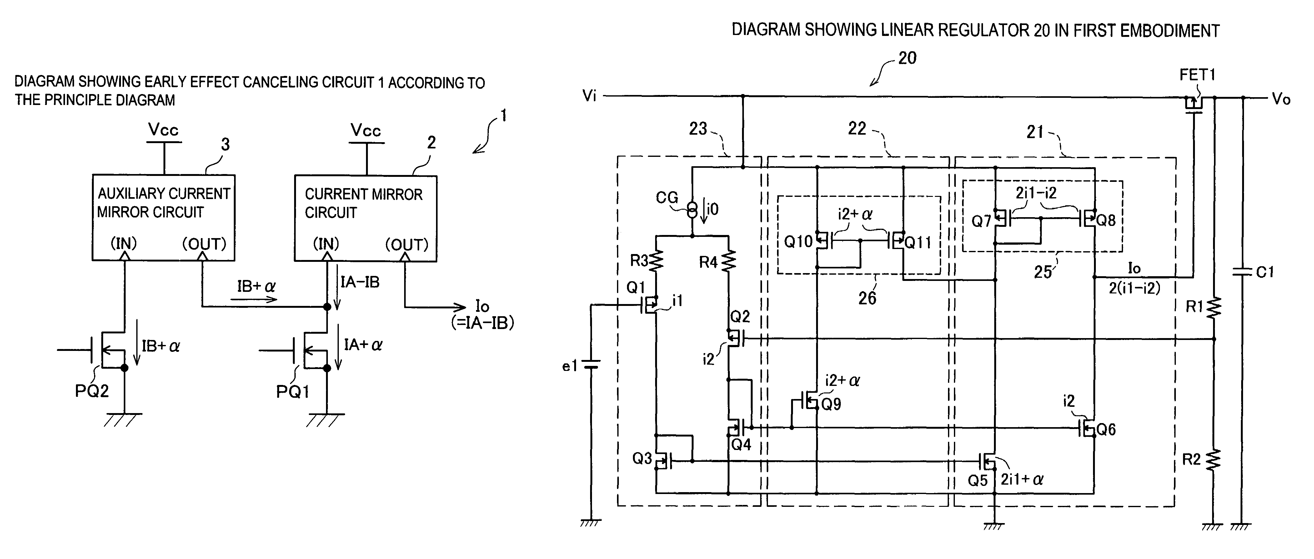
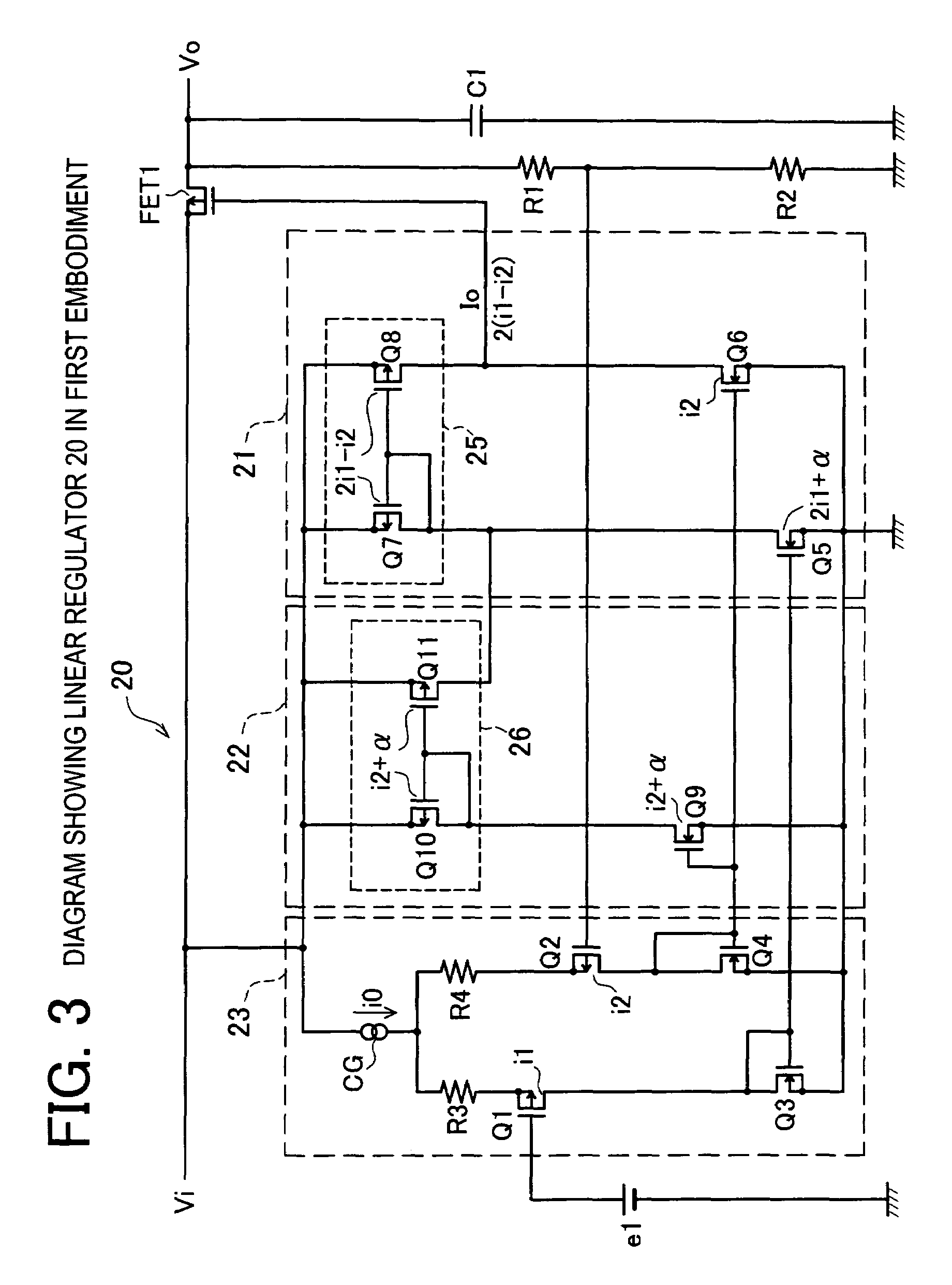
[0039]In the first embodiment, cancelation of Early voltage effects in driver circuit 21 is explained by referring to FIG. 3. The linear regulator 20 shown in FIG. 3 comprises a driver circuit 21, an Early voltage detector 22, an error amplifier 23, a main transistor FET1, a capacitor C1, and resistance elements R1 and R2. The linear regulator 20 receives an input voltage Vi, and sends out an output voltage Vo. The main transistor FET1 is a transistor for regulating the input voltage Vi, and issuing an output voltage Vo. The input voltage Vi is put in the source electrode of the main transistor FET1, and the output voltage Vo is issued from the drain electrode. An output terminal of the driver circuit 21 is connected to the control electrode (gate) of the main transistor FET1. The capacitor C1 is a capacitor for smoothing the output voltage Vo.
[0040]The driver circuit 21 is a circuit for driving the main transistor FET1 by receiving the output of the error amplifier 23. The driver c...
second embodiment
[0076]A linear regulator 20a in the second embodiment is explained by referring to FIG. 5. Early voltage effects appear in inverting input side transistor Q1 to which reference voltage e1 of error amplifier 23 is connected, and noninverting input side transistor Q2 receiving divided voltage of output voltage Vo. Hence, the linear regulator 20a has first auxiliary error amplifier 24 and second auxiliary error amplifier 34 in parallel to each input. Hence, this is a method of preventing Early voltage effects from appearing in output current of error amplifier 23.
[0077]The first auxiliary error amplifier 24 and second auxiliary error amplifier 34 are a differential input current mirror circuit composition having a same element configuration as the error amplifier 23. The first auxiliary error amplifier 24 is connected in parallel to the inverting input side transistor Q1 of the error amplifier 23, and second auxiliary error amplifier 34 is connected in parallel to the noninverting inpu...
PUM
 Abstract
Description
Claims
Application Information


