Three-dimensional device fabrication method

a fabrication method and three-dimensional technology, applied in semiconductor devices, semiconductor/solid-state device details, electrical devices, etc., can solve the problems of severely limited performance of microprocessors, restrictions on the amount of cache memory, etc., and achieve the effect of relaxed requirements for wafer flatness and highly precise alignment between wafers

Inactive Publication Date: 2008-04-08
IBM CORP
View PDF28 Cites 214 Cited by
  • Summary
  • Abstract
  • Description
  • Claims
  • Application Information

AI Technical Summary

Benefits of technology

[0006]According to the present invention, the vias in the respective wafers need not extend vertically from the front surface to the back surface of the wafers. A conducting body, provided in the wafer beneath the device region and extending laterally, may connect the via with the metallized opening in the back surface. Accordingly, the conducting path through the wafer may be led underneath the devices thereof. The bonding layer is preferably a thermoplastic material, and in particular may be polyimide. This permits wafers to be bonded with less stringent requirements regarding flatness and cleanliness.

Problems solved by technology

If both the logic unit and the memory devices of a microprocessor are arranged in a two-dimensional (2-D) pattern, limitations on the physical size of the chip (imposed by poor process yields for large-area chips) may lead to restrictions on the amount of cache memory.
The performance of the microprocessor may therefore be severely limited.
Significant problems in the present state of the art of 3-D integration include (1) the need for reliable wafer bonding; (2) stringent wafer cleanliness and flatness requirements; (3) the need for reliable, low-resistance inter-wafer vertical connections; (4) stringent wafer-to-wafer lateral registration requirements; and (5) the need for efficient heat conduction through the 3-D device.

Method used


Image

  • Three-dimensional device fabrication method
  • Three-dimensional device fabrication method
  • Three-dimensional device fabrication method

Examples


Embodiment Construction

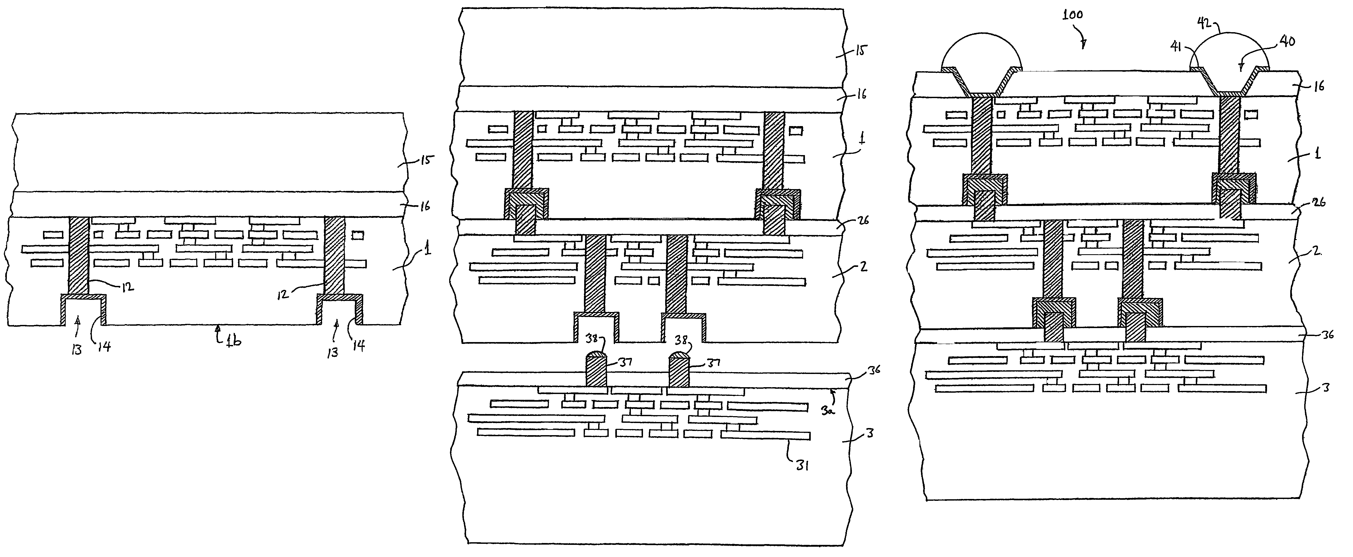
[0015]In accordance with the present invention, a plurality of thinned wafers with devices formed thereon may be stacked and vertically interconnected. In the embodiments described herein, a three-level stack is fabricated and connected; it will be appreciated that this is for illustration purposes only, and that the process may be adapted to more or fewer than three levels. The 3-D, vertically integrated device may be constructed in two ways, as detailed below.

(1) Top-down Wafer Stack Process

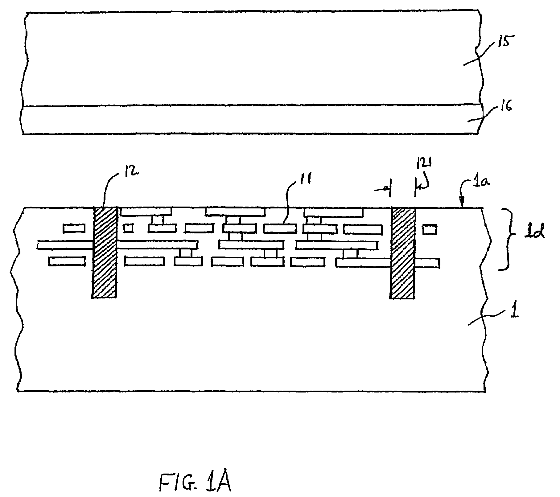
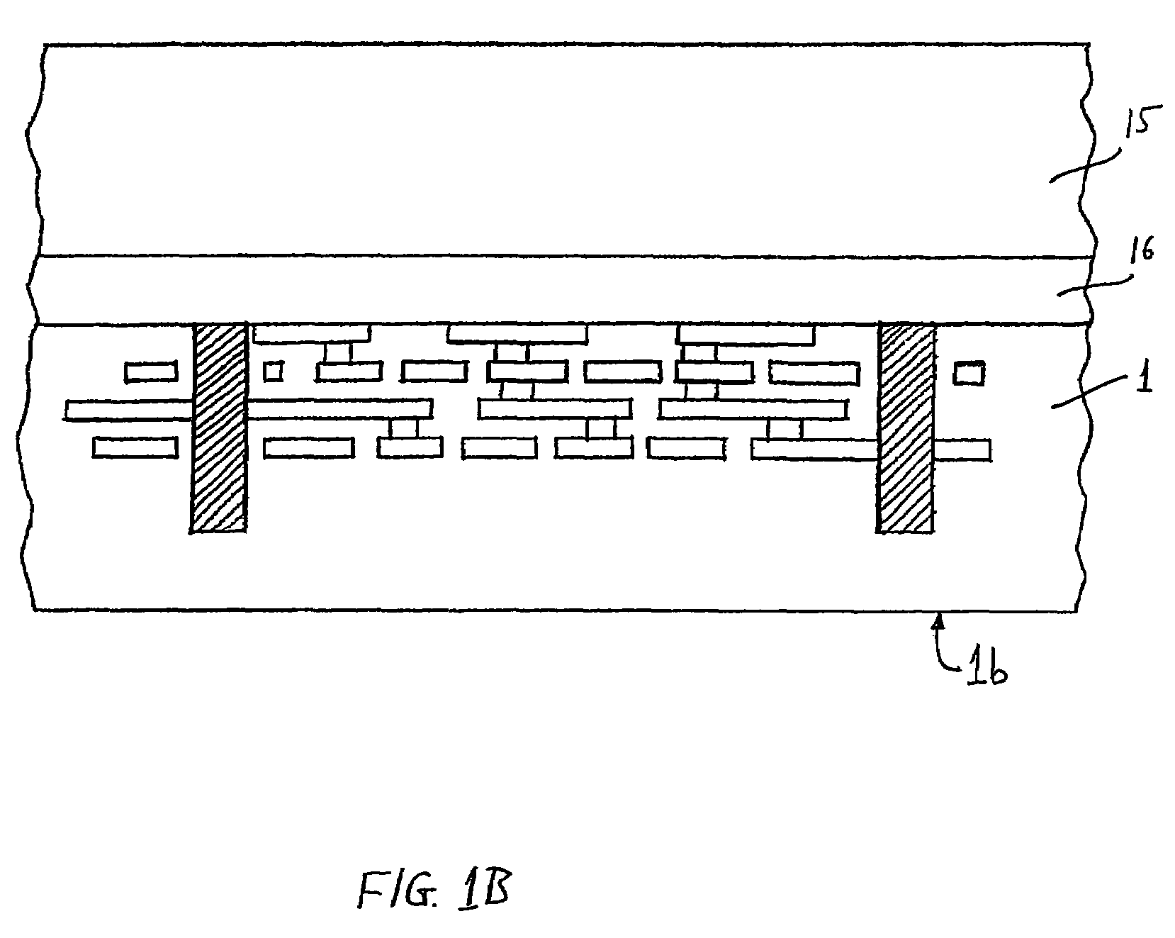
[0016]FIG. 1A shows in cross-section a wafer 1 having devices and several levels of high-density interconnection wiring 11 (typically Cu) in a region 1d of the wafer near the front surface 1a thereof Metallized vias 12 are formed in the wafer, extending below the region 1d of devices and lateral interconnects; these vias will become part of the vertical through-connections after wafer 1 is thinned. Vias 12 are typically formed by etching holes in wafer 1, forming a layer of liner material on th...


PUM


Abstract

A method is described for fabricating a three-dimensional integrated device including a plurality of vertically stacked and interconnected wafers. Wafers (1, 2, 3) are bonded together using bonding layers (26, 36) of thermoplastic material such as polyimide; electrical connections are realized by vias (12, 22) in the wafers connected to studs (27, 37). The studs connect to openings (13, 23) having a lateral dimension larger than that of the vias at the front surfaces of the wafers. Furthermore, the vias in the respective wafers need not extend vertically from the front surface to the back surface of the wafers. A conducting body (102) provided in the wafer beneath the device region and extending laterally, may connect the via with the matallized opening (103) in the back surface. Accordingly, the conducting path through the wafer may be led underneath the devices thereof. Additional connections may be made between openings (113) and studs (127) to form vertical heat conduction pathways between the wafers.

Description

FIELD OF THE INVENTION[0001]This invention relates to the manufacture of very large-scale integrated semiconductor devices, and more particularly to methods for fabricating three-dimensional, vertically interconnected chips.BACKGROUND OF THE INVENTION[0002]Microprocessor chips generally include a logic unit and cache memory. If both the logic unit and the memory devices of a microprocessor are arranged in a two-dimensional (2-D) pattern, limitations on the physical size of the chip (imposed by poor process yields for large-area chips) may lead to restrictions on the amount of cache memory. The performance of the microprocessor may therefore be severely limited.[0003]To address the problem of providing adequate cache memory for microprocessors (and more generally the problem of 2-D real estate on a chip), a number of researchers are exploring methods for building three-dimensional (3-D) integrated circuits. A typical 3-D fabrication process includes building devices on wafers which a...

Claims


Application Information

Patent Timeline
Patent Type & Authority Patents(United States)
IPC IPC(8): H01L21/46H01L21/00H01L21/4763
CPCH01L21/6835H01L23/481H01L24/16H01L24/81H01L24/83H01L25/0652H01L25/0657H01L25/50H01L21/568H01L24/03H01L24/05H01L24/06H01L24/13H01L24/14H01L24/17H01L24/29H01L24/32H01L24/92H01L2221/68327H01L2221/6834H01L2221/68359H01L2221/68381H01L2224/02372H01L2224/03002H01L2224/0345H01L2224/03849H01L2224/05569H01L2224/0557H01L2224/05571H01L2224/05572H01L2224/06519H01L2224/131H01L2224/13111H01L2224/13144H01L2224/14519H01L2224/16146H01L2224/16147H01L2224/16225H01L2224/17519H01L2224/2919H01L2224/32145H01L2224/32225H01L2224/73104H01L2224/73204H01L2224/81005H01L2224/81141H01L2224/81191H01L2224/81192H01L2224/81203H01L2224/81385H01L2224/81815H01L2224/83191H01L2224/83203H01L2224/8385H01L2224/92H01L2225/06513H01L2225/06517H01L2225/06541H01L2225/06593H01L2924/01013H01L2924/01029H01L2924/01047H01L2924/01057H01L2924/01079H01L2924/01082H01L2924/15311H01L2924/01006H01L2924/01019H01L2924/01033H01L2924/0105H01L2924/01074H01L2924/014H01L2924/0132H01L2224/29111Y10S438/977H01L2924/15192H01L2224/0401H01L2924/0002H01L2224/81H01L2224/83H01L2924/00014H01L2924/00H01L2224/13116H01L2924/00012H01L2924/0695H01L2224/05552H01L2924/14H01L2224/16145H01L21/50
Inventor POGGE, H. BERNHARDYU, ROY
Owner IBM CORP
Why Eureka
Try Eureka