LED chip-containing photonic crystal side direction light extractor

A technology of light-emitting diodes and light extractors, applied in semiconductor devices, electrical components, circuits, etc., can solve the problems of large heat generation and stress concentration, and achieve the effects of stable performance, high luminous brightness, and improved external quantum efficiency.

Active Publication Date: 2009-06-03
HC SEMITEK SUZHOU
View PDF0 Cites 6 Cited by
  • Summary
  • Abstract
  • Description
  • Claims
  • Application Information

AI Technical Summary

Problems solved by technology

[0003] In order to overcome the above problems, the object of the present invention is to provide a light-emitting diode chip with a photonic crystal side light extractor, which is used to improve the light extraction efficiency of the chip and the large heat generation and stress caused by the excessive size of some chips. Concentration etc.

Method used


Image

  • LED chip-containing photonic crystal side direction light extractor
  • LED chip-containing photonic crystal side direction light extractor
  • LED chip-containing photonic crystal side direction light extractor

Examples


Embodiment Construction

[0041] Below according to accompanying drawing and embodiment the present invention is described in further detail.

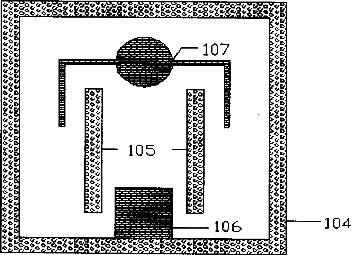
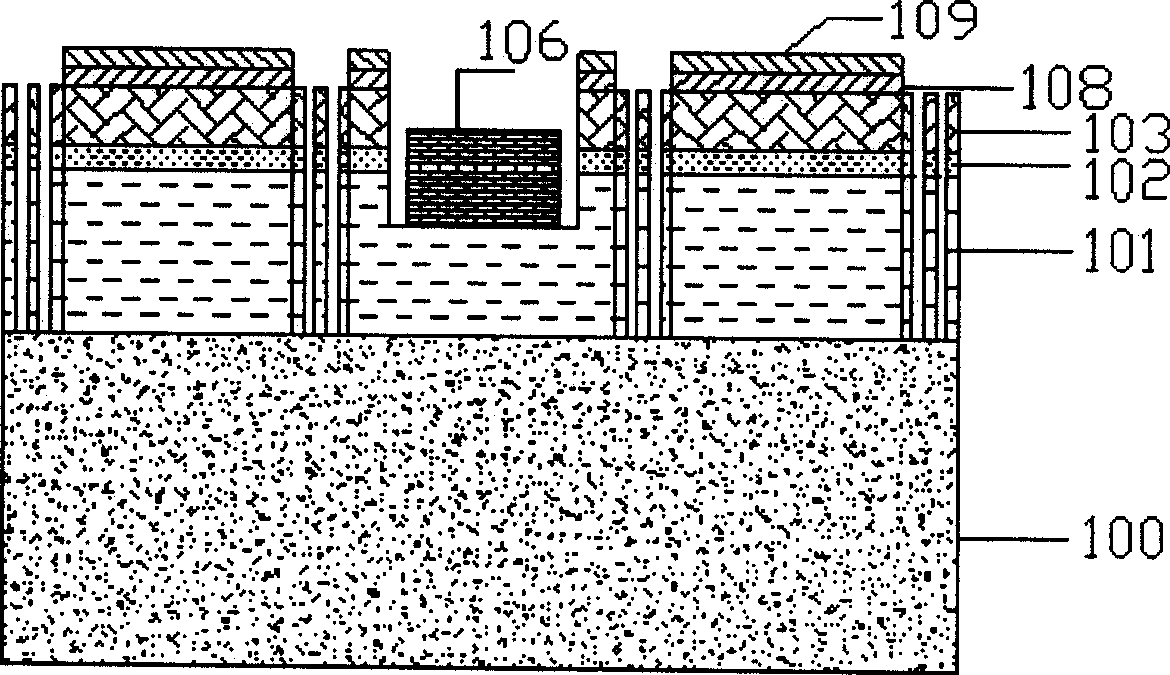
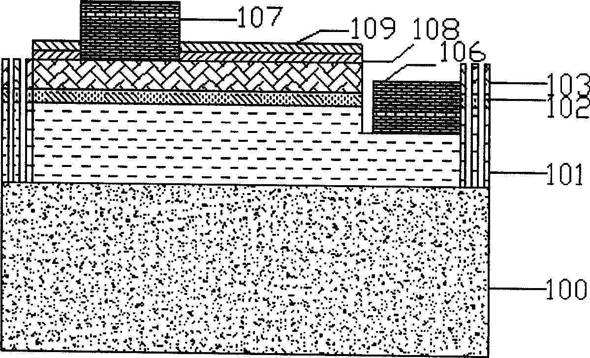
[0042] Figure 1A ~ Figure 1C Explanation of middle marks: 100—substrate, 101—n pole region, 102—active layer, 103—p pole region, 104—surrounding pillar array, 105—middle pillar array, 106—N electrode, 107—P electrode, 108— Current spreading layer, 109—protective layer.

[0043] Figure 2A ~ Figure 2IExplanation of middle marks: 200—substrate, 201—n pole region, 202—active layer, 203—p pole region, 204—passivation layer, 205—photoresist, 206—N electrode, 207—P electrode, 208— Current spreading layer, 209—protective layer.

[0044] see Figure 1A ~ Figure 1C , are top view, front view and side view of Embodiment 1 of the present invention.

[0045] see Figure 1A , is a top view of Embodiment 1 of the present invention, showing the relative positions of the peripheral column array 104 and the middle column array 105, the N electrode 106 and the P electrode 1...


PUM


Abstract

An LED chip-containing photonic crystal side direction light extractor comprises a substrate, an n-pole area, an active layer and a p-pole area, wherein, an N electrode is arranged on the n-pole area; a P electrode and a current-diffusing layer are arranged on the p-pole area; and a protective layer is arranged on the current-diffusing layer. The chip is characterized in that: the photonic crystal side direction light extractor comprises a column array; the column arrays penetrate the p-pole area, the active layer and the n-pole area to the surface of the substrate; the photonic crystal side direction light extractor comprises the column array which is arranged on the circumference of the chip and a column array which is arranged in the middle of the chip; and the current-diffusing layer between the N electrode and the P electrode keeps an electric conduction pathway. As the photonic crystal side direction light extractor is arranged to revise the light angle, the chip further has the advantage that more lateral optical is project to the outside, thereby greatly improving the external quantum efficiency of an LED, overcoming the problems that the light taking efficiency of a chip is low; the stress is centralized; the calorific value is big; and the radiating effect is poor. Therefore, the produced LED has the advantages that the performance is stabler; and the luminance is even larger.

Description

technical field [0001] The invention relates to the field of semiconductor optoelectronic devices, in particular to a light emitting diode chip with a photonic crystal side light extractor and a manufacturing method thereof, which are used to improve the chip light extraction efficiency and luminous brightness. Background technique [0002] A light emitting diode (LED) is a semiconductor light emitting device with high photoelectric conversion efficiency. With the continuous progress of semiconductor preparation technology and the development and utilization of new materials, GaN-based blue LEDs have gradually matured. External quantum efficiency is the main technical bottleneck of high-brightness LED chips. At present, the internal quantum efficiency of commercial LEDs has reached over 90%, while the external quantum efficiency is only 3-30%, which is mainly due to the low escape rate of light. The factor causing the low escape rate of light is mainly due to the relativel...

Claims


Application Information

Patent Timeline
Patent Type & Authority Applications(China)
IPC IPC(8): H01L33/00
Inventor 张建宝林波涛
Owner HC SEMITEK SUZHOU
Why Eureka
Try Eureka