Method for manufacturing semiconductor device

a manufacturing method and semiconductor technology, applied in the direction of semiconductor devices, basic electric elements, electrical equipment, etc., can solve the problems of difficult use of increase in number of steps, and difficulty in using integrated circuits including thin films, so as to achieve efficient and massively small manufacturing devices

Active Publication Date: 2008-04-08
SEMICON ENERGY LAB CO LTD
View PDF13 Cites 100 Cited by
  • Summary
  • Abstract
  • Description
  • Claims
  • Application Information

AI Technical Summary

Benefits of technology

[0015]It is an object of the present invention to provide a method for manufacturing efficiently and massively very small devices which can receive or transmit data in touch, preferably, out of touch by forming a thin film integrated circuit over a large glass substrate and peeling the integrated circuit from the substrate. Especially, the thin film integrated circuit is difficult to use since there is a threat that the integrated circuit is flied when being transported since the integrated circuit is extremely thin.
[0018]Consequently, the inventors find that the generation of a fissure in an integrated circuit can be prevented when the proceeding of etching is controlled in the case of providing a peeling layer over a substrate, providing a peeled layer including an integrated circuit over the peeling layer, and removing the peeling layer by etching.
[0033]In this specification, the term “laminate film” denotes a stacked film including a base film and an adhesive synthetic resin film or a stacked film including two or more kinds of layers. As the base film, polyester such as PET or PBT, polyamide such as nylon 6 or nylon 66, an inorganic deposited film, or papers may be used. As an adhesive synthetic resin film, polyolefin such as PE or PP, acrylic-based synthetic resin, epoxy-based synthetic resin, or the like may be used. A laminate film is laminated by thermocompressing to an object using a laminating device. As pretreatment for a laminate step, an anchor coat agent is preferably coated, which can strengthen the adhesiveness between the laminate film and an object. Isocyanate-based material or the like may be used as the anchor coat agent.
[0037]According to the invention, damage such as a fissure to a semiconductor integrated circuit can be reduced.

Problems solved by technology

Especially, the thin film integrated circuit is difficult to use since there is a threat that the integrated circuit is flied when being transported since the integrated circuit is extremely thin.
However, the number of steps increases when another substrate is used, and transferring step is required one more time.
Especially, the integrated circuit including a thin film is difficult to use since the integrated circuit is extremely thin.

Method used


Image

  • Method for manufacturing semiconductor device
  • Method for manufacturing semiconductor device
  • Method for manufacturing semiconductor device

Examples


embodiment mode 1

[0059]Here, a method for manufacturing a semiconductor device according to the present invention is explained hereinafter.

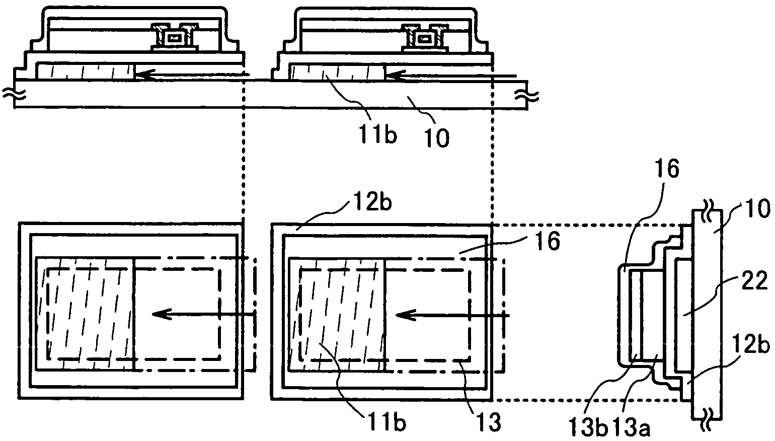
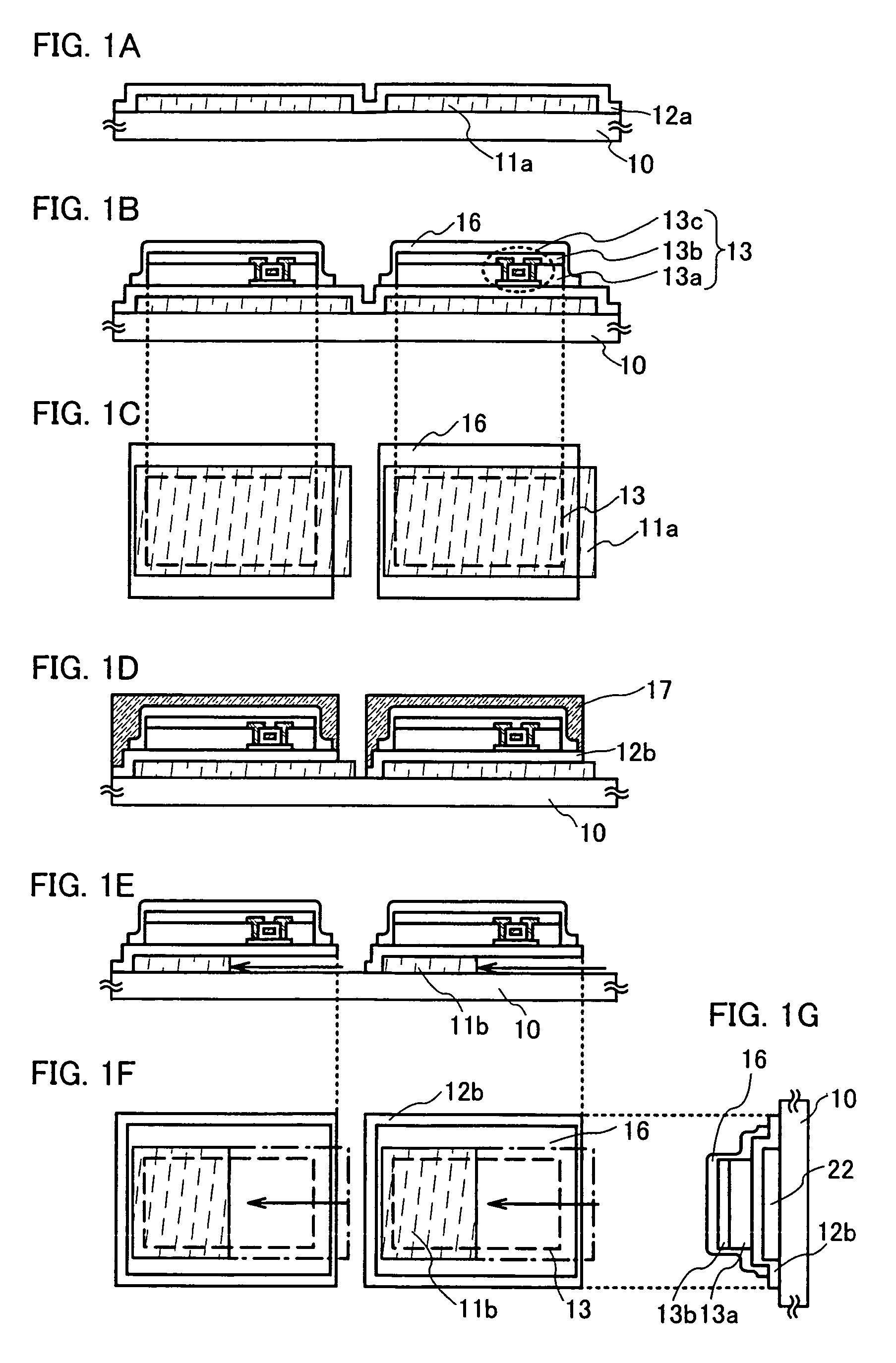
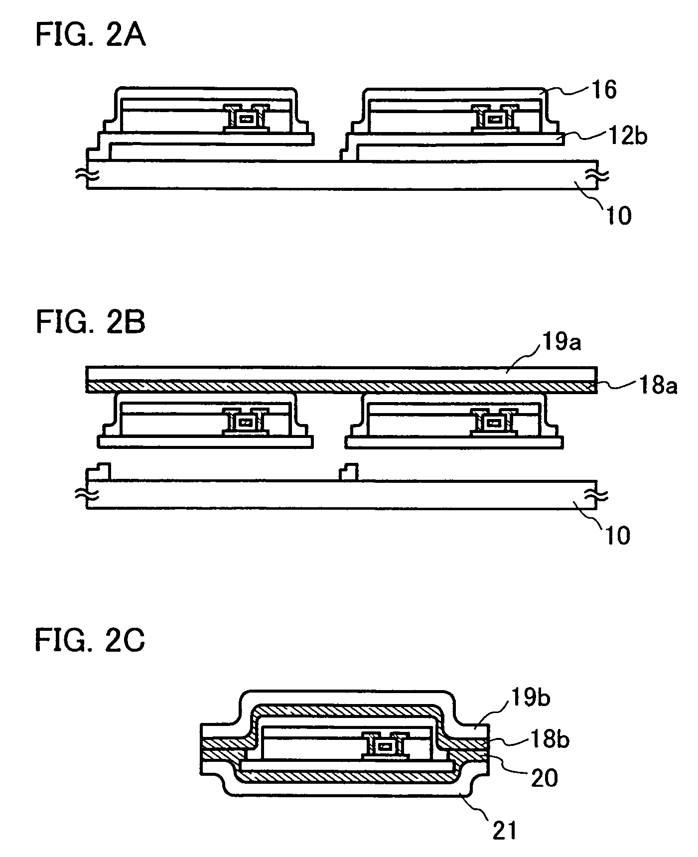
[0060]First, a peeling layer 11a is formed over a substrate 10 having an insulating surface, patterning of the peeling layer is performed. The substrate 10 having the insulating surface corresponds to a glass substrate, a quartz substrate, a plastic substrate, a resin substrate formed from a flexible synthetic resin such as acrylic, or a metal substrate. As for the peeling layer 11a, a layer containing silicon is formed by a known method such as a sputtering method or a plasma CVD method. The layer containing silicon corresponds to an amorphous semiconductor layer, a semi-amorphous semiconductor layer in which an amorphous state and a crystalline state are mixed, or a crystalline semiconductor layer.

[0061]Then, a base insulating layer 12a including an inorganic insulating film is formed. As for the base insulating layer 12a, a single layer film including silicon ...

embodiment mode 2

[0075]Here, a manufacturing method which is different from that of Embodiment Mode 1 is explained with reference to FIGS. 3A to 3F.

[0076]First, an island-shaped peeling layer 311a is formed over a substrate 310 having an insulating surface in the similar way as in Embodiment Mode 1. Then, a base insulating layer 312a including an inorganic insulating film is formed in the similar way as in Embodiment Mode 1 (refer to FIG. 3A).

[0077]Then, a peeled layer 313 including a first element group and the base insulating layer 312a as the first layer is formed in the similar way as in Embodiment Mode 1. The peeled layer 313 including the first element group includes a first interlayer insulating layer 313a, a second interlayer insulating layer 313b, a plurality of TFTs 313c, and a conductive layer serving as an antenna. The peeled layer 313 including the first element group ends up being one device. Then, a protective layer 316 is formed by a screen printing method or a droplet discharge meth...

embodiment mode 3

[0086]Here, a manufacturing method which is different from those in Embodiment Mode 1 and Embodiment Mode 2 is explained with reference to FIGS. 4A to 5B.

[0087]Embodiment Mode 1 illustrates an example in which a peeling layer is formed in an island shape; however, this embodiment mode illustrates an example without patterning a peeling layer.

[0088]First, a peeling layer 411a is formed over the whole surface of a substrate 410 having an insulating surface. Then, a base insulating layer 412a including an inorganic insulating film is formed (refer to FIG. 4A).

[0089]A peeled layer 413 including a first element group and the base insulating layer 412a as the first layer is formed. The peeled layer 413 including the first element group includes a first interlayer insulating layer 413a, a second interlayer insulating layer 413b, a plurality of TFTs 413c, and a conductive layer serving as an antenna. The peeled layer 413 including the first element group ends up being one device.

[0090]Then,...


PUM


Abstract

In the case where an integrated circuit formed of a thin film is formed over a substrate and peeled from the substrate, a fissure (also referred to as crack) is generated in the integrated circuit in some cases. The present invention is to restrain the generation of a fissure by fixing the proceeding direction of etching in one direction to make a peeled layer warp in one direction in accordance with the proceeding of etching. For example, the proceeding of etching can be controlled by utilizing the fact that a portion where a substrate is in contact with a base insulating layer is not etched in the case of patterning a peeling layer provided over the substrate, then forming the base insulating layer, and then fixing a peeled layer by the portion where the substrate is in contact with the base insulating layer.

Description

BACKGROUND OF THE INVENTION[0001]1. Field of the Invention[0002]The present invention relates to a semiconductor device comprising a circuit including a thin film transistor (hereinafter, referred to as TFT) and a method for manufacturing the semiconductor device. For example, the invention relates to an electronic device on which an electro-optical device as typified by a liquid crystal display panel or a light emitting display device having an organic light emitting element is mounted as a component.[0003]Further, in this specification, the term “semiconductor device” denotes a device in general which can operate by utilizing a semiconductor characteristic. An electro-optical device, a semiconductor circuit, and an electronic device are all included in the semiconductor device.[0004]2. Description of the Related Art[0005]In recent years, technique of forming a thin film transistor (TFT) using a semiconductor thin film (having a thickness of approximately from several to several hu...

Claims


Application Information

Patent Timeline
Patent Type & Authority Patents(United States)
IPC IPC(8): H01L21/44
CPCH01L21/7806H01L27/1214H01L27/1266
Inventor SUGIYAMA, EIJIITO, KYOSUKE
Owner SEMICON ENERGY LAB CO LTD
Why Eureka
Try Eureka