Configurable width buffered module having a bypass circuit

a bypass circuit and module technology, applied in memory systems, memory subsystems, memory modules or systems having memory devices, etc., can solve the problem that memory systems also require high throughput for bandwidth intensive applications

Inactive Publication Date: 2008-04-08
RAMBUS INC
View PDF163 Cites 67 Cited by
  • Summary
  • Abstract
  • Description
  • Claims
  • Application Information

AI Technical Summary

Problems solved by technology

In addition to upgradeability, many of these contemporary memory systems also require high throughput for bandwidth intensive applications, such as graphics.

Method used


Image

  • Configurable width buffered module having a bypass circuit
  • Configurable width buffered module having a bypass circuit
  • Configurable width buffered module having a bypass circuit

Examples


Embodiment Construction

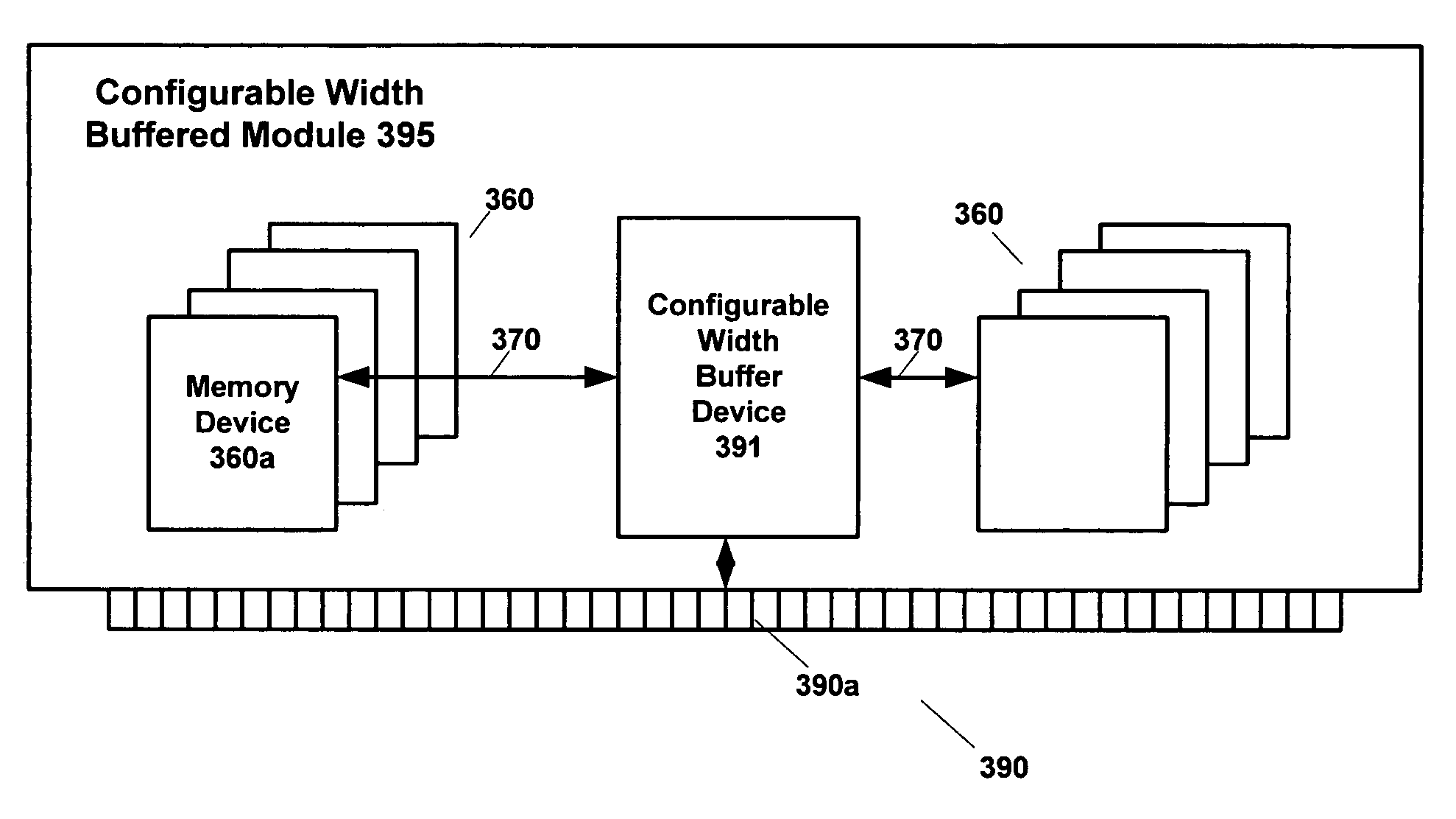
[0045]The present invention relates to a memory system which includes one or more semiconductor memory devices coupled to a buffer device having a bypass circuit. The buffer device may be disposed on a memory module, housed in a common package along with memory devices, or situated on a motherboard, for example, main memory in a personal computer or server. The buffer device may also be employed in an embedded memory subsystem, for example such as one found on a computer graphics card, video game console or a printer.

[0046]In several embodiments, the buffer device having a bypass circuit provides for flexible system configurations, and several performance benefits. For example, a buffer device having a bypass circuit enables adding memory module upgrades to a memory system while reducing system delays for accessing information from the memory module upgrades. Further, the buffer device may be a configurable width buffer device to provide upgrade flexibility and / or provide high bandw...


PUM


Abstract

A memory system architecture / interconnect topology includes a configurable width buffered memory module having a configurable width buffer device with at least one bypass circuit. A buffer device, such as a configurable width buffer device, is positioned between or with at least one integrated circuit memory device positioned on a substrate surface of a memory module, such as a DIMM. The configurable width buffer device is coupled to at least one memory device (by way of an internal channel), entry pin and exit pin on the memory module. The configurable width buffer device includes a multiplexer / demultiplexer circuit coupled to the entry pin and the internal channel for accessing the memory device. A bypass circuit is coupled to the entry pin and the exit pin in order to allow information to be transferred through the memory module to another coupled memory module in the memory system by way of an external channel. In an alternate embodiment of the present invention, two bypass circuits are coupled to a pair of entry and exit pins. In an embodiment of the present invention, a memory system may include at least four interfaces, or sockets, for respective memory modules having configurable width buffer devices with bypass circuits that enable additional upgrade options while reducing memory system access delays.

Description

[0001]This application is a continuation-in-part of U.S. patent application Ser. No. 10 / 766,131 filed on Jan. 28, 2004 (still pending); which is a continuation-in-part of U.S. patent application Ser. No. 10 / 272,024 filed on Oct. 15, 2002 (still pending); which is a continuation of U.S. patent application Ser. No. 09 / 479,375 filed on Jan. 5, 2000 (now U.S. Pat. No. 6,502,161).BACKGROUND OF THE INVENTION[0002]This invention relates to memory systems, memory subsystems, memory modules or a system having memory devices. More specifically, this invention is directed toward memory system architectures that may include integrated circuit devices such as one or more controllers and a plurality of memory devices.[0003]Some contemporary memory system architectures may demonstrate tradeoffs between cost, performance and the ability to upgrade, for example; the total memory capacity of the system. Memory capacity is commonly upgraded via memory modules or cards featuring a connector / socket inte...

Claims


Application Information

Patent Timeline
Patent Type & Authority Patents(United States)
IPC IPC(8): G06F12/00G06F13/16G11C5/00G11C29/02
CPCG06F13/1684G11C5/04G11C29/02G11C29/028G11C29/50012G11C2029/1806H05K1/181
Inventor PEREGO, RICHARDWARE, FREDTSERN, ELYHAMPEL, CRAIG
Owner RAMBUS INC
Why Eureka
Try Eureka