Wide spatial frequency topography and roughness measurement

a topography and spatial frequency technology, applied in the field of wide spatial frequency topography and roughness measurement, can solve the problems of failure of a hard disk, high cost, and inability to retrieve data,

Inactive Publication Date: 2008-04-22
KLA TENCOR TECH CORP
View PDF4 Cites 41 Cited by
  • Summary
  • Abstract
  • Description
  • Claims
  • Application Information

AI Technical Summary

Problems solved by technology

One problem that the manufacturers of hard disks experience is how to maximize the operating life of a hard disk.
When a hard disk fails the data stored therein may be difficult, expensive, or impossible to retrieve.
Failure of a hard disk may be caused by defects on the surface of the thin film disk.
As a result even very small defects can cause a hard drive to fail.
The problem is that the CMP process can leave residual copper, nitride, or CMP slurry on the surface of the wafer.
In addition, stains, particles, scratches, and micro-waviness may be present on the polished wafer.
Fewer defects will also mean greater wafer yields at the end of the process.
A problem in the hard disk, semiconductor and photonics industries is to inspect these magnetic disks and wafers for defects such as particles, scratches, pits, mounds, stains, topographic irregularities and inclusions.
None of these systems enables the simultaneous measurement of topographic and non-topographic defects.

Method used


Image

  • Wide spatial frequency topography and roughness measurement
  • Wide spatial frequency topography and roughness measurement
  • Wide spatial frequency topography and roughness measurement

Examples


Embodiment Construction

[0030]A preferred embodiment of the present invention is now described with reference to the figures where like reference numbers indicate identical or functionally similar elements. Also in the figures, the left most digit(s) of each reference number correspond(s) to the figure in which the reference number is first used.

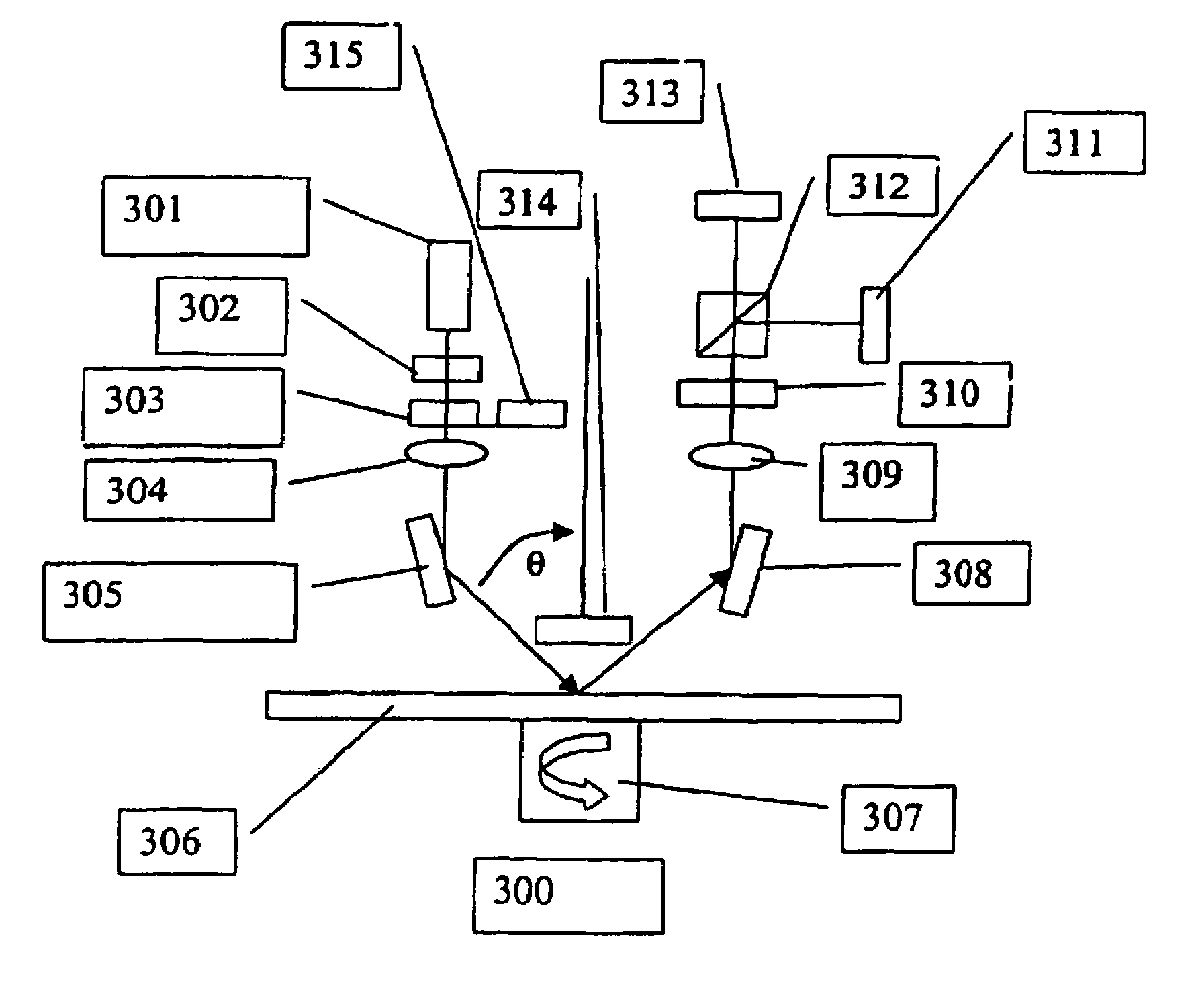
[0031]FIG. 3 is an illustration of an apparatus for measuring properties of the thin film according to an embodiment of the present invention. The apparatus uses a focused laser light signal whose angle of propagation θ (as shown in FIG. 3) can be between zero degrees from normal and ninety degrees from normal.

[0032]One embodiment of the apparatus 300 includes a conventional laser diode 301, e.g., RLD65MZT1 or RLD-78MD available from Rolm Corporation, Kyoto, Japan, which has been collimated by Hoetron Corp., Sunnyvale, Calif., e.g., a conventional linear polarizer 302, e.g., made of Polarcor that is commercially available from Newport Corp., Irvine, Calif., a conve...


PUM

PropertyMeasurementUnit
thicknessaaaaaaaaaa
angle of propagationaaaaaaaaaa

Abstract

In one embodiment, a system to inspect a surface comprises an assembly to direct a first radiation beam onto a surface in a first plane of incidence, a first detector to generate a first signal from a portion of the radiation reflected from the first radiation beam, a first spatial filter interposed between the surface and the first detector, a first ellipsoidal mirror to collect scattered light, a second detector to generate a second signal from the scattered portion of the beam, and a processor to generate, from the first and second signals, a data set representing one or more characteristics of the surface using the first and second signals.

Description

RELATED APPLICATIONS[0001]This application is continuation-in-part of 11 / 268,214 (U.S. Pat. Ser. No. 7,110,097), entitled Combined High Speed Optical Profilometer and Ellipsometer, by Steven W. Meeks, et al., filed Nov. 7, 2005, which is a continuation of co-pending, commonly assigned U.S. patent application Ser. No. 10 / 873,892 (U.S. Pat. No. 7,075,630), entitled Combined High Speed Optical Profilometer and Ellipsometer, by Steven W. Meeks, et al., filed Jun. 21, 2004, which is a continuation of patent application Ser. No. 09 / 861,280 (U.S. Pat. No. 6,757,056), entitled “Combined High Speed Optical Profilometer And Ellipsometer”, that was filed on May 18, 2001 (U.S. Pat. No. 6,757,056) and claims priority under 35 U.S.C. §120 to U.S. patent application Ser. No. 09 / 818,199, entitled “A combined High speed Optical Profilometer and Ellipsometer”, that was filed on Mar. 26, 2001, all of which are incorporated by reference in their entirety.BACKGROUND[0002]1. Field of the Invention[0003]T...

Claims


Application Information

Patent Timeline
Patent Type & Authority Patents(United States)
IPC IPC(8): G01N21/00
CPCG01B11/303G01N21/9501
Inventor MEEKS, STEVEN W.RAMACHANDRAN, MAHENDRA PRABHUMOGHADAM, ALIREZA SHAHDOOST
Owner KLA TENCOR TECH CORP
Why Eureka
Try Eureka