Electro-optical device, film member, laminated film, low refractivity film, laminated multilayer film and electronic appliances

a technology of electronic devices and film members, applied in the field of electronic devices, can solve problems such as display quality degradation, and achieve the effect of excellent display quality

Inactive Publication Date: 2008-04-22
ELEMENT CAPITAL COMMERCIAL CO PTE LTD
View PDF47 Cites 20 Cited by
  • Summary
  • Abstract
  • Description
  • Claims
  • Application Information

AI Technical Summary

Benefits of technology

[0009]An object of the present invention carried out considering the situations above is to provide an electro-optical device that can realize high display quality by improving the projection efficiency of the light while maintaining sealing ability of the element.
[0037]According to the present invention, electronic appliances having excellent display quality and being able to retain desired functions for a long period of time can be realized.

Problems solved by technology

Since the projection efficiency of the light is poor, only a part of the light can contribute to display even when a prescribed intensity of an electric current is supplied to the luminous layer 102, causing a deterioration of the display quality.

Method used


Image

  • Electro-optical device, film member, laminated film, low refractivity film, laminated multilayer film and electronic appliances
  • Electro-optical device, film member, laminated film, low refractivity film, laminated multilayer film and electronic appliances
  • Electro-optical device, film member, laminated film, low refractivity film, laminated multilayer film and electronic appliances

Examples


first embodiment

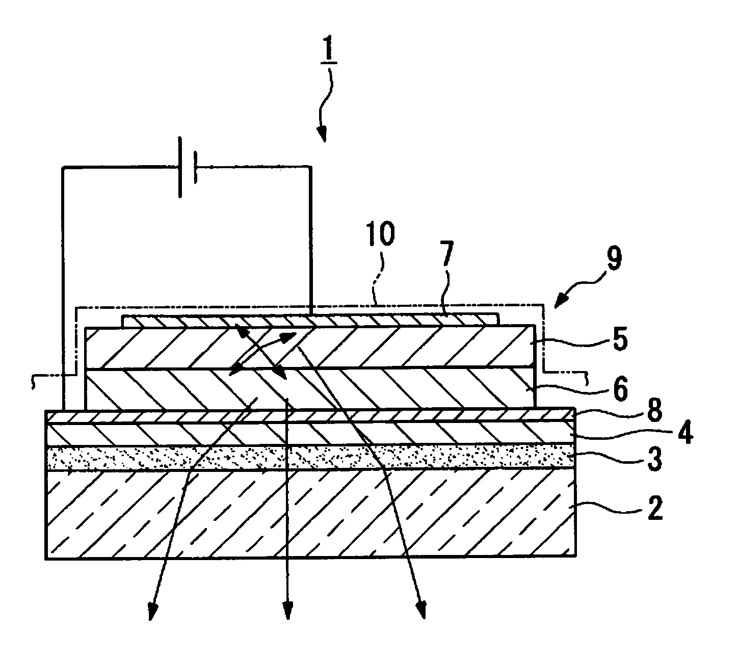
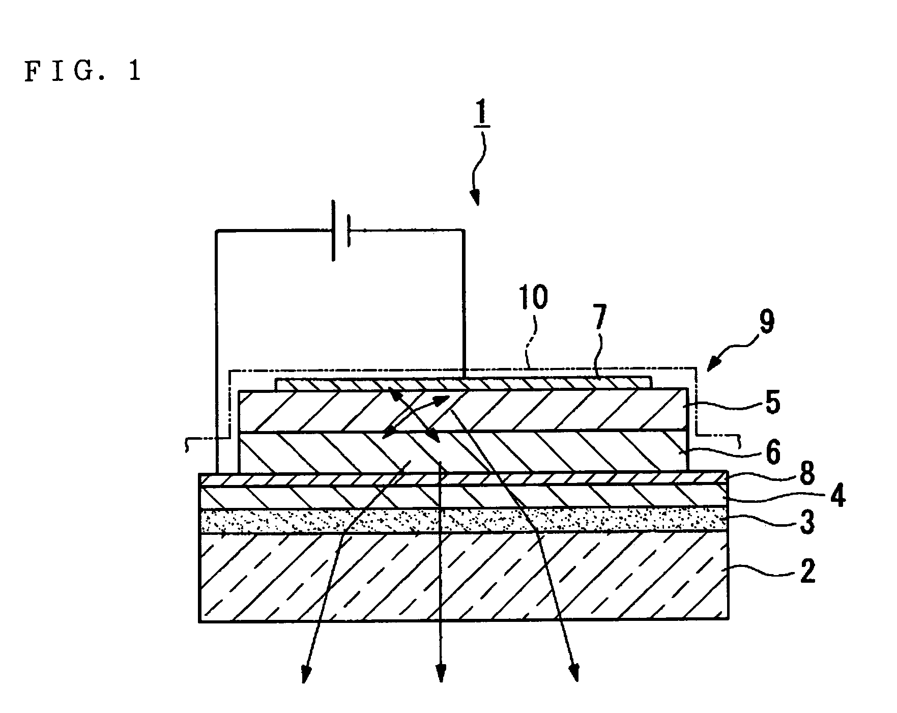
[0056]The electro-optical device according to the present invention will be described hereinafter with reference to FIG. 1. FIG. 1 is a cross section showing an example of an organic electroluminescence display as the electro-optical device according to the present invention.

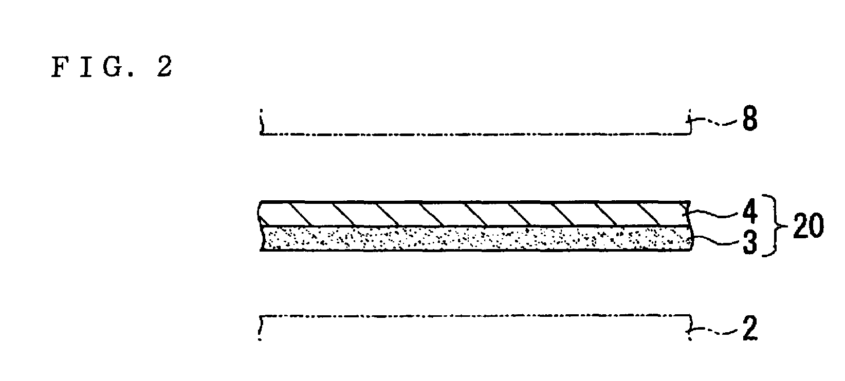
[0057]As shown in FIG. 1, the organic electroluminescence display 1 can include a light permeable substrate (light transmission layer) 2, an organic electroluminescence element (luminous element) 9 having a luminous layer 5 and positive hole transfer layer 6 made of an organic electroluminescent material interposed between a pair of negative electrode (cathode) 7 and positive electrode (anode) 8 provided at one face side of the substrate 2, and a low refractivity film 3 and seal layer 4 laminated between the substrate 2 and organic electroluminescence element 9. The low refractivity film 3 can be provided at the substrate side relative to the seal layer 4.

[0058]As shown in FIG. 1, the light emitted from the lumi...

third embodiment

[0101]The construction of the electro-optical device according to the present invention as a third embodiment will be described hereinafter with reference to FIGS. 4, 5 and 6. FIGS. 4 and 5 show an example when the electro-optical device according to the present invention is applied to an active matrix type display.

[0102]The organic luminescence display S1 includes a plurality of scanning lines 131, a plurality of signal lines 132 elongating in a direction perpendicular to the scanning lines 131, and a plurality of common power lines 133 elongating in parallel to the signal lines 132 disposed on a substrate. A pixel (pixel region) AR is provided at each cross point between the scanning lines 131 and signal lines 132.

[0103]A data line addressing circuit 90 includes a shift resistor, level shifter, video line and analogue switch is provided for the signal lines 132.

[0104]A scanning line addressing circuit 80 having a shift resistor and level shifter is provided, on the other hand, for...

second embodiment

[0188]The low refractivity film 3 and seal layer 4 are formed on the surface of the negative electrode 222. Since these low refractivity film 3 and seal layer 4, and the method for forming them are equivalent to those in the first and second embodiment, descriptions thereof will be omitted herein.

[0189]As described above, recognition of vision is largely improved while preventing gases that cause the element to be deteriorated from invading by applying the laminated film 20 according to the present invention to the top emission type electro-optical device.

[0190]It is naturally possible to apply the low refractivity film 11 containing the drying agent or adsorbent as described in the second embodiment, in place of the laminated film 20 shown in FIG. 6.

[0191]A hole blocking layer may be formed at the opposed electrode 222 side to the luminous layer 60 in place of the positive hole injection / transfer layer 70, luminous layer 60 and electron transfer layer 50, in order to prolong the se...


PUM


Abstract

The invention provides an electro-optical device capable of improving a high light projection efficiency to the outside while maintaining sealing ability for providing high recognition of vision. An organic electroluminescence display can include a light permeable substrate, and an organic electroluminescence element having a luminous layer and positive hole transfer layer interposed between a pair of electrodes. Additionally, a low refractivity film having a lower refractivity than the substrate, and a seal layer for blocking the air from invading from the substrate side to the organic electroluminescence element are laminated between the substrate and electrode of the organic electroluminescence element.

Description

[0001]This is a Division of application Ser. No. 10 / 285,546 filed Nov. 1, 2002 now U.S. Pat. No. 6,985,275. The entire disclosure of the prior application is hereby incorporated by reference herein in its entirety.BACKGROUND OF THE INVENTION[0002]1. Field of Invention[0003]The present invention relates to an electro-optical device, a film member suitably provided in the electro-optical device, laminated film, low refractivity film, laminated multilayer film and electronic appliances comprising the electro-optical device.[0004]2. Description of Related Art[0005]An electroluminescence display (electro-optical device) including an organic electroluminescence element corresponding to each pixel has excellent display performance due to its highly luminous spontaneous light emission, capability of addressing by low current density and voltage, as well as high speed response and emission by a solid organic layer. Such a display is expected to be the successor of a liquid crystal display in...

Claims


Application Information

Patent Timeline
Patent Type & Authority Patents(United States)
IPC IPC(8): G02B1/10H01L51/50H01L51/52H05B33/04H05B33/22
CPCH01L51/5237H01L51/5262H10K59/873H10K59/874H05B33/22H10K50/85H10K50/844H10K50/846
Inventor MIYAZAWA, TAKASHI
Owner ELEMENT CAPITAL COMMERCIAL CO PTE LTD
Why Eureka
Try Eureka