Semiconductor device with semiconductor components connected to one another

a semiconductor and semiconductor technology, applied in the direction of instruments, final product manufacturing, sustainable manufacturing/processing, etc., can solve the problems of limiting transmission speed, adversely affecting signal transmission, and multiple intermediate contact-connections with parasitic capacitances

Inactive Publication Date: 2008-04-29
POLARIS INNOVATIONS
View PDF11 Cites 11 Cited by
  • Summary
  • Abstract
  • Description
  • Claims
  • Application Information

AI Technical Summary

Benefits of technology

[0009]It is an object of the present invention to provide a semiconductor device which

Problems solved by technology

This disadvantageously gives rise to a multiplicity of intermediate contact-connections with parasitic capacitances.
This results in connecting lengths in the range of many millimeters, with the disadvantageous properties of a high capacitance and a high inductance.
The large number of contact-connection transitions adversely influences the signal transmission; in particular, it limits the transmission speed.
A further s

Method used


Image

  • Semiconductor device with semiconductor components connected to one another
  • Semiconductor device with semiconductor components connected to one another
  • Semiconductor device with semiconductor components connected to one another

Examples


Embodiment Construction

[0028]Identical reference symbols designate identical or functionally identical devices.

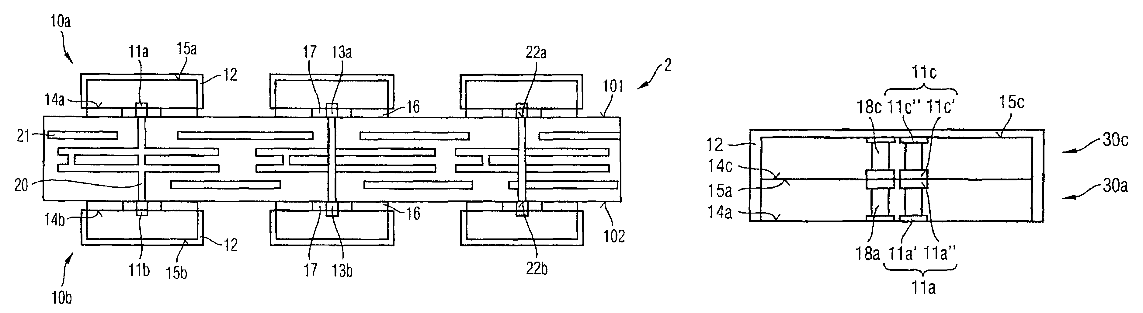
[0029]FIG. 1 illustrates a schematic illustration of a first embodiment of the present invention. A substrate 2 is provided, which has an internal wiring device 21 within it and in part also on its first contact-connection side 101 and on its second contact-connection side 102 opposite to the first contact-connection side 101. The substrate 2 is advantageously a multilayer printed circuit board. However, the substrate 2 may also be formed from a semiconductor substrate with a corresponding wiring device.

[0030]The substrate 2 has one or more contact-connection areas 22a on the first contact-connection side 101, which are connected via a vertical through-plating device 20 to second contact-connection areas 22b on the second contact-connection side 102 of the substrate 2. The first 22a and second contact-connection areas 22b are arranged in a manner lying opposite one another.

[0031]One or more unhou...


PUM


Abstract

The present invention relates to a semiconductor device which provides a shortest possible connection between two semiconductor components 10a and 10b arranged in a manner lying opposite on a substrate 2. The two semiconductor components 10a and 10b are in each case arranged with their chip contact-connection regions 11a and 11b facing the substrate 2. A vertical through-plating device 20 connects the two chip contact-connection regions 11a and 11b.

Description

DESCRIPTION[0001]1. Technical Field[0002]The present invention relates to a semiconductor device with semiconductor components connected to one another.[0003]2. Background Art[0004]Although the present invention is described below with regard to modules comprising semiconductor memory components on a multilayer printed circuit board, the invention is not restricted thereto.[0005]Memory components are expediently combined to form larger modules by a plurality of memory components being mounted on a multilayer printed circuit board. A larger storage capacity of a module is achieved in this way. A typical arrangement of such a module is shown by way of example in FIG. 7. Memory components 1a and 1b are mounted on both sides on a multilayer printed circuit board 2. The memory components typically have a housing and external contact-connections 9. Within the housing, the memory components 1a and 1b are connected by their chip contact-connection regions 4 to the external contact-connectio...

Claims


Application Information

Patent Timeline
IPC IPC(8): H01L23/48H01L23/52H01L29/40
CPCG11C5/04H01L23/481H01L23/5383H01L23/5384H01L24/16H01L24/31H01L25/0652H05K1/181H01L2224/16235H01L23/3114H01L2224/13099H01L2224/16225H01L2224/48091H01L2224/48227H01L2924/01005H01L2924/01078H01L2924/01079H01L2924/12044H01L2924/15311H01L2924/30107H01L2924/3011H05K3/429H05K2201/10545H05K2201/10674H01L21/563H01L2924/12041H01L2924/014H01L2924/01006H01L24/48H01L2924/00014H01L2924/00H01L2224/0554H01L2224/0557H01L2224/05571H01L2224/05573H01L2924/181Y02P70/50H01L2224/05599H01L2924/00012H01L2224/45099H01L2224/45015H01L2924/207H01L2224/0555H01L2224/0556
Inventor HEDLER, HARRYMUFF, SIMON
Owner POLARIS INNOVATIONS
Why Eureka
Try Eureka