
Logical-to-physical lane assignment to reduce clock power dissipation in a bus having a variable link width
a technology of logical-to-physical lane assignment and bus power dissipation, which is applied in the direction of electric digital data processing, instruments, climate sustainability, etc., can solve the problems of reducing the battery life of mobile computers, reducing the power consumption of buses, and undesirable high-power consumption. achieve the effect of reducing the power of buses
- Summary
- Abstract
- Description
- Claims
- Application Information
AI Technical Summary
Benefits of technology
Problems solved by technology
Method used
Image

Examples
Embodiment Construction
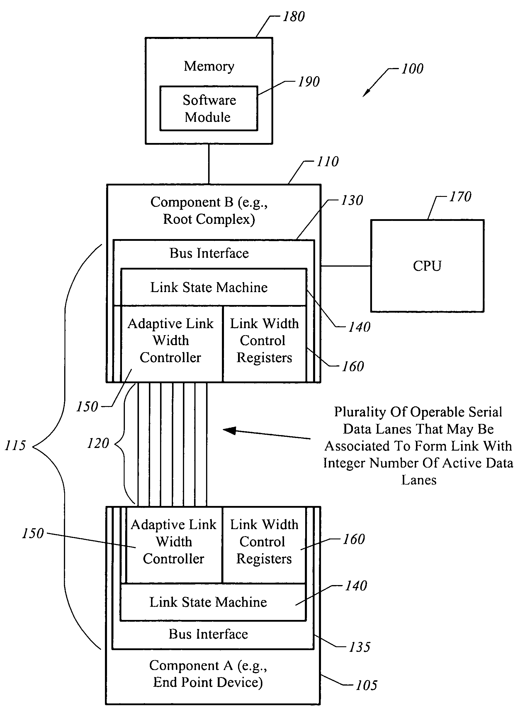
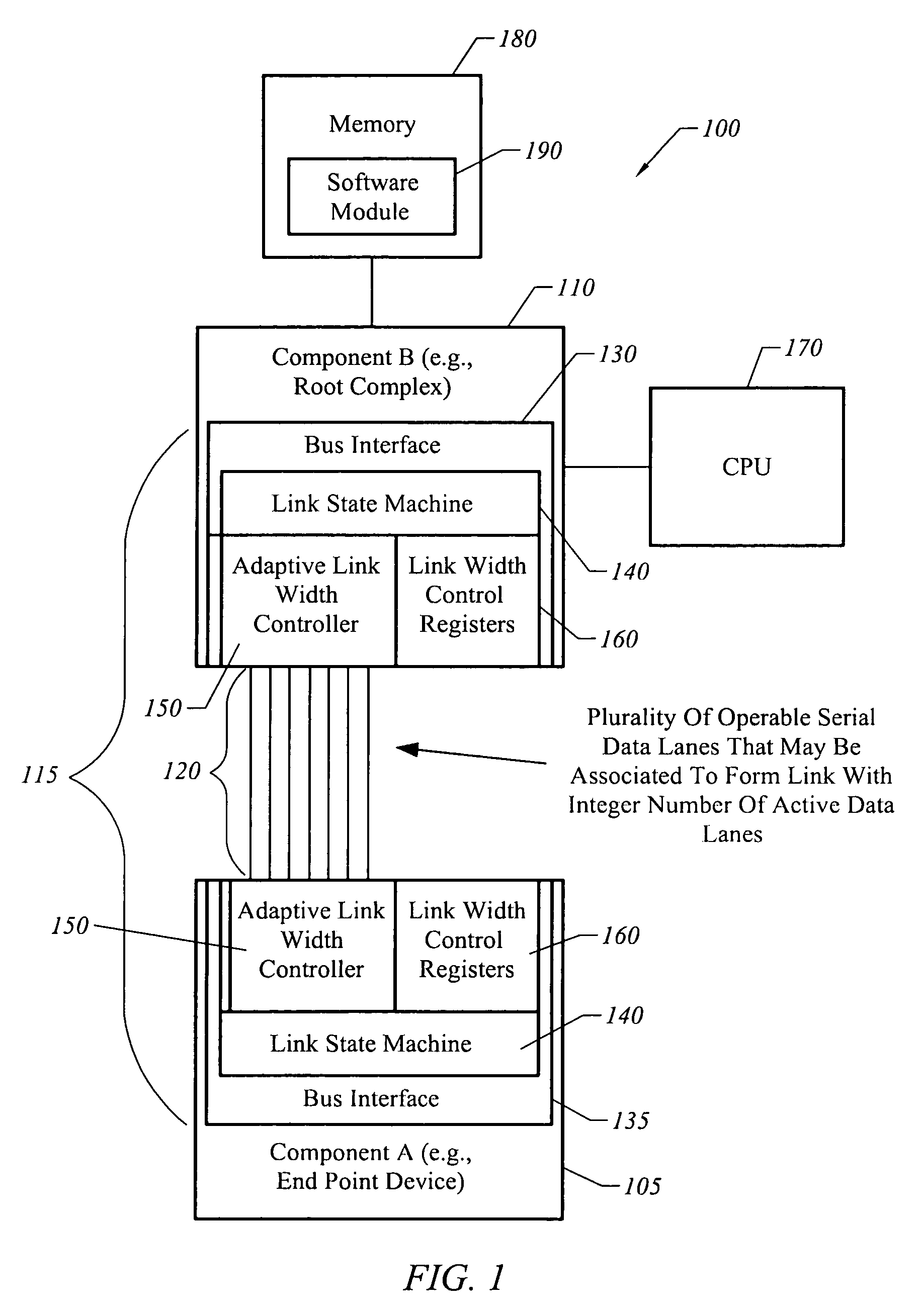
[0034]The present invention is directed towards an apparatus, system, and method for adaptively adjusting bus bandwidth. FIG. 1 is an illustrative block diagram of a system 100 in accordance with one embodiment of the present invention. Referring to FIG. 1, system 100 includes two components 105 and 110 that are communicatively coupled by a data bus 115 comprised of a plurality of serial data lanes 120 and bus interfaces 130 and 135.
[0035]In some embodiments, bus 115 is part of a system in which a first component 105 is an end-point device, such as a graphical processing unit (GPU). The other component 110 may correspond to a bridge, such as a root complex for peripheral devices. A CPU 170 and memory 180 having executable software instructions 190 may be coupled to component 110. However, it will be understood in the following description that bus 115 may be utilized in a variety of systems other than that illustrated in FIG. 1.
[0036]In one embodiment, each of the serial data lanes ...
PUM
 Abstract
Description
Claims
Application Information