Bus switch circuit and interactive level shifter

a switch circuit and level shifter technology, applied in the field of bus switch circuits and interactive level shifters, can solve the problems of signal delay, low propagation speed between terminals a and b, increase in cost,

Inactive Publication Date: 2008-05-13
KK TOSHIBA
View PDF10 Cites 25 Cited by
  • Summary
  • Abstract
  • Description
  • Claims
  • Application Information

AI Technical Summary

Benefits of technology

[0016]A bus switch circuit according to an aspect of the present invention comprises a switch element which has two terminals connected between first and second terminals and whose electrical connection is controlled when a control signal is input to a control terminal, a first pull-up resistor and first switch circuit connected in series between a power supply voltage terminal and the first terminal, and a second pull-up resistor and second switch circuit connected in series between the power supply voltage terminal and the second terminal, wherein electrical connection of the first switch circuit is controlled upon receiving the control signal, when the switch element is turned on, the first switch circuit is turned on to connect the power supply voltage terminal to the first terminal through the first pull-up resistor, and when the switch element is turned off, the first switch circuit is turned off to disconnect the power supply voltage terminal from the first terminal, and electrical connection of the second switch circuit is controlled upon receiving the control signal, when the switch element is turned on, the second switch circuit is turned on to connect the power supply voltage terminal to the second terminal through the second pull-up resistor, and when the switch element is turned off, the second switch circuit is turned off to disconnect the power supply voltage terminal from the second terminal.
[0017]An interactive level shifter according to an aspect of the present invention comprises a level shift section which receives a power supply voltage and outputs a first power supply voltage lower by a predetermined voltage, a control signal generation section which receives the first power supply voltage and outputs a first control signal having the power supply voltage at high level and a second control signal having the first power supply voltage at high level, a switch element having two terminals connected between first and second terminals and whose electrical connection is controlled when the second control signal is input to a control terminal, and a pull-up resistor and switch circuit connected in series between a power supply voltage terminal and the second terminal, wherein electrical connection of the switch circuit is controlled upon receiving the first control signal, when the switch element is turned on, the switch circuit is turned on to connect the power supply voltage terminal to the second terminal through the pull-up resistor, and when the switch element is turned off, the switch circuit is turned off to disconnect the power supply voltage terminal from the second terminal.
[0018]An interactive level shifter according to another aspect of the present invention comprises a level shift section which receives a power supply voltage and outputs a first power supply voltage lower by a predetermined voltage, a control sign...

Problems solved by technology

However, the conventional bus switch circuit has the following problem.
However, the above-described conventional interactive level shifter has the following problems.
The two kinds of power supply voltages VccA and VccB are necessary for level shift, resulting in an increase in cost.
In addition, since each of the circuits CT1 and CT2 and logic level converter LLC is constituted by a logic circuit with a...

Method used


Image

  • Bus switch circuit and interactive level shifter
  • Bus switch circuit and interactive level shifter
  • Bus switch circuit and interactive level shifter

Examples


first embodiment

(1) First Embodiment

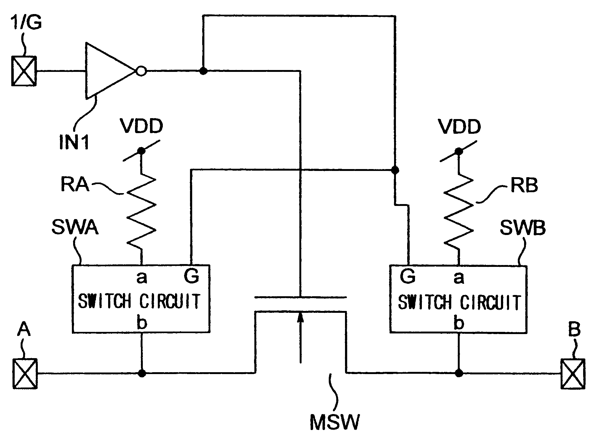
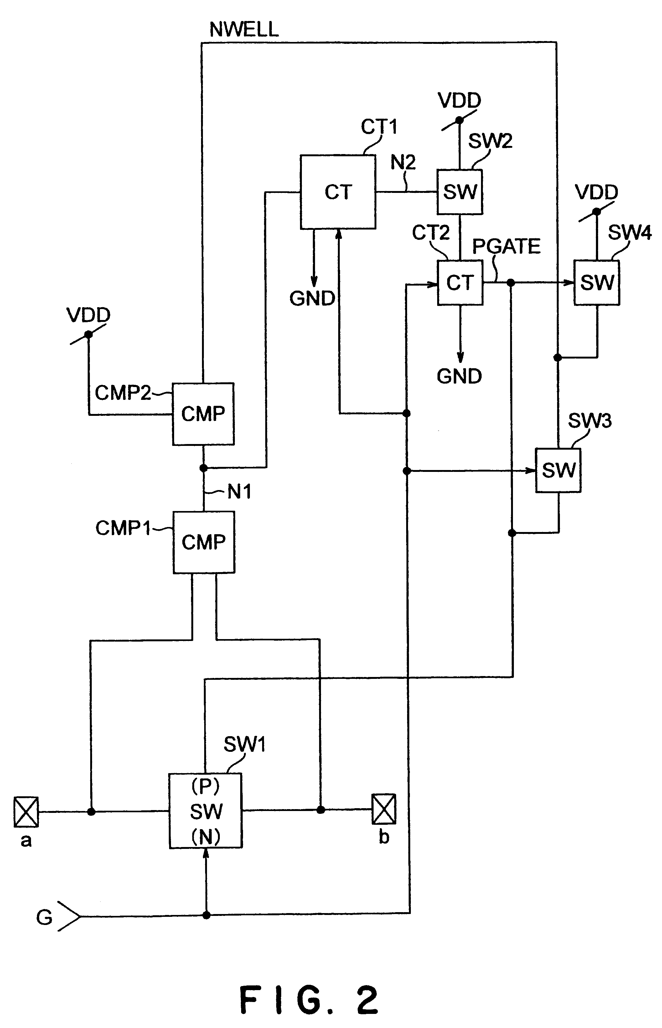
[0050]FIG. 2 shows the detailed circuit arrangement of a switch circuit SWA or SWB according to the first embodiment of the present invention.

[0051]A switch element SW1 having a CMOS structure formed from a p-channel transistor and n-channel transistor is connected between terminals a and b. The n-channel transistor is turned on / off by a control signal G (switch enable at high level and switch disable at low level). The p-channel transistor whose gate receives a gate signal PGATE is turned on in the switch enable mode and off in the switch disable mode, like the n-channel transistor.

[0052]The terminals a and b are connected to a comparator CMP1. The potentials of the terminals a and b are compared, and a higher potential is output to a node N1.

[0053]A comparator CMP2 compares the potential of the node N1 with a power supply voltage VDD. When the potential of the node N1 is equal to or higher than the power supply voltage VDD, the node N1 and n-well NWELL are conn...

second embodiment

(2) Second Embodiment

[0074]FIG. 3 shows the detailed circuit arrangement of a switch circuit SWA or SWB according to the second embodiment of the present invention.

[0075]The sources and drains of a p-channel transistor TR1 and n-channel transistor TR2, which form a switch element SW1, are connected between terminals a and b. The gate of the transistor TR1 is connected to a node PGATE. A control signal G is input to the gate of the transistor TR2.

[0076]The terminals of p-channel transistors TR3 and TR4 and n-channel transistor TR5 are connected in series between a power supply voltage VDD terminal and a ground terminal. The gate of the transistor TR3 is connected to a node P1. The control signal G is input to the gates of the transistors TR3 to TR5.

[0077]One terminal of a p-channel transistor TR6 is connected to an n-well NWELL. The control signal G is input to the gate of the transistor TR6. The other terminal is connected to the node PGATE.

[0078]One terminal of a p-channel transist...

third embodiment

(3) Third Embodiment

[0111]As another example of switch circuit SWA or SWB shown in FIG. 1, the third embodiment of the present invention will be described with reference to FIG. 4.

[0112]One terminal and the other terminal of each of p-channel transistor TR21 and n-channel transistor TR22 of the switch element of a CMOS circuit are connected in parallel between terminals a and b. A control signal G is input to the gate of the transistor TR22. The gate of the transistor TR21 is connected to a node GB.

[0113]The potential of the node GB is determined by the ON / OFF states of transistors TR25 and TR26. The terminals of the p-channel transistor TR25 and n-channel transistor TR26 are connected in series between an n-well NWELL1 and a ground terminal.

[0114]The potential of the node GB, which is determined by inputting the control signal G to the gates of the transistors TR25 and TR26, is input to the gate of the transistor TR21, thereby controlling electrical connection.

[0115]The terminals o...


PUM


Abstract

A bus switch circuit includes a switch element having two terminals whose electrical connection is controlled when a control signal is input into a control terminal. The bus switch circuit further includes a first pull-up resistor and first switch circuit, a second pull-up resistor and second switch circuit. The control signal controls the electrical connections of the first and second switch circuits.

Description

CROSS-REFERENCE TO RELATED APPLICATION[0001]This application claims benefit of priority under 35 USC 119 to Japanese Patent Application No. 2001-219975, filed on Jul. 19, 2001, and No. 2001-220033, filed on Jul. 19, 2001, the entire contents of which are incorporated by reference herein.BACKGROUND OF THE INVENTION[0002]The present invention relates to a bus switch circuit and an interactive level shifter.[0003]In recent years, bus switch circuits are used in many products. For example, when first and second circuits which operate upon receiving a power supply voltage are connected, a bus switch circuit is used to, e.g., block the signal path to prevent any operation error caused when a signal output from the first circuit is input to the second circuit before the power supply voltage is supplied to the second circuit.[0004]FIG. 10 shows the arrangement of a conventional bus switch circuit. The source and drain of a switch element SW formed from an n-channel transistor are connected ...

Claims


Application Information

Patent Timeline
IPC IPC(8): H03K19/0175G06F1/32H03K17/06H03K19/0185H04L12/50
CPCG06F1/3203G06F1/3253H03K19/018507H03K17/063Y02B60/1235Y02D10/00
Inventor FUKUOKA, MASATOSASHIHARA, FUMIO
Owner KK TOSHIBA
Why Eureka
Try Eureka