
Plasma display panel having scan electrode closer to address electrode

a display panel and scan electrode technology, applied in the direction of address electrodes, static indicating devices, instruments, etc., can solve the problems of reducing driving efficiency, reducing discharge-sustain and discharge firing voltages, etc., to improve driving efficiency, improve structure, and reduce address voltage

Inactive Publication Date: 2008-05-20
SAMSUNG SDI CO LTD
View PDF6 Cites 0 Cited by
  • Summary
  • Abstract
  • Description
  • Claims
  • Application Information

AI Technical Summary

Benefits of technology

[0021]The present invention provides a PDP having an improved structure that may increase driving efficiency by reducing an address voltage.
[0022]The present invention also provides a PDP that may reduce a discharge sustaining voltage.
[0023]The present invention also provides a PDP having improved brightness and image definition since a sufficient amount of meta-stable particles that allow for a decreased driving voltage may be attained even with fine discharge cells.

Problems solved by technology

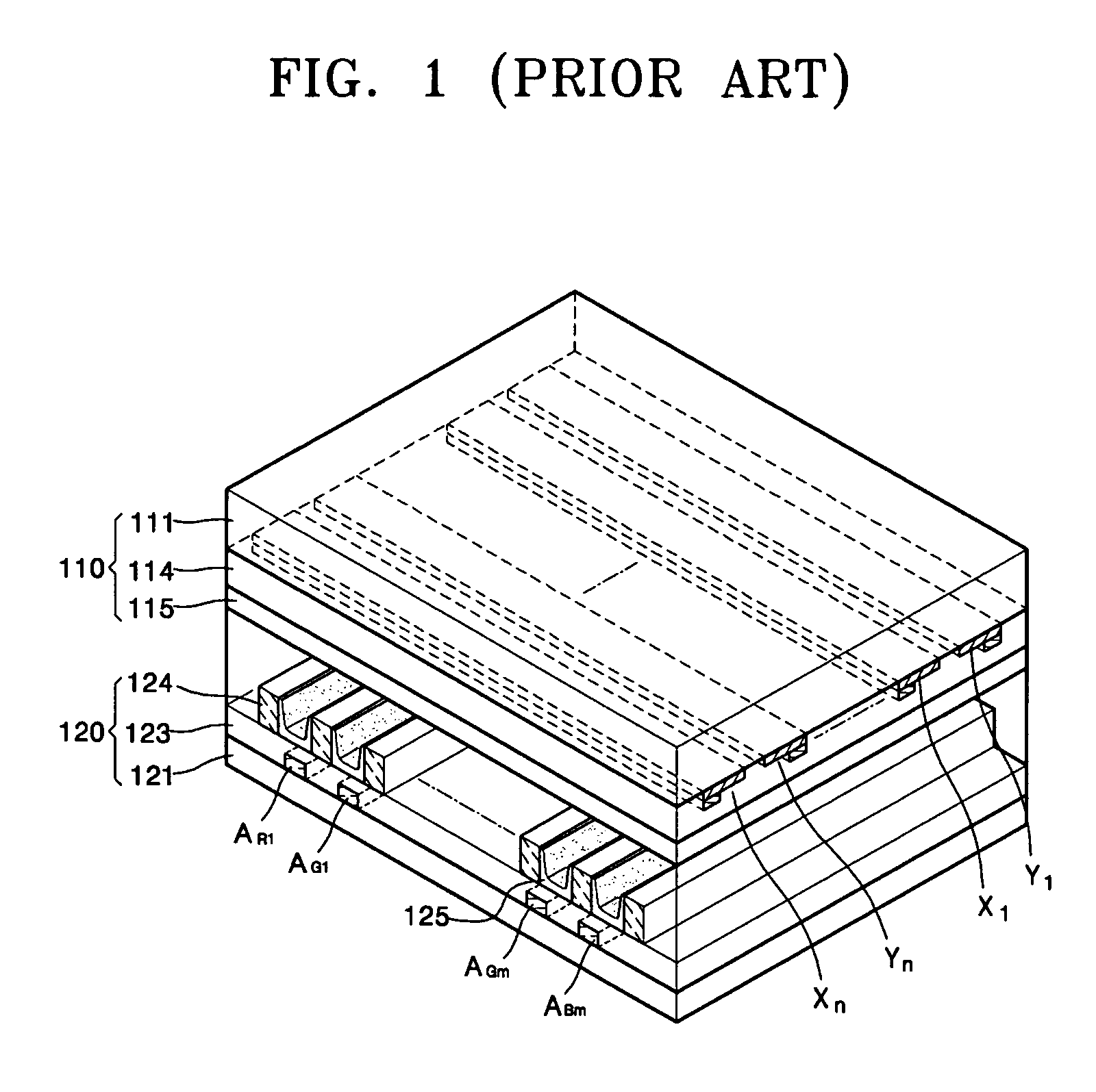
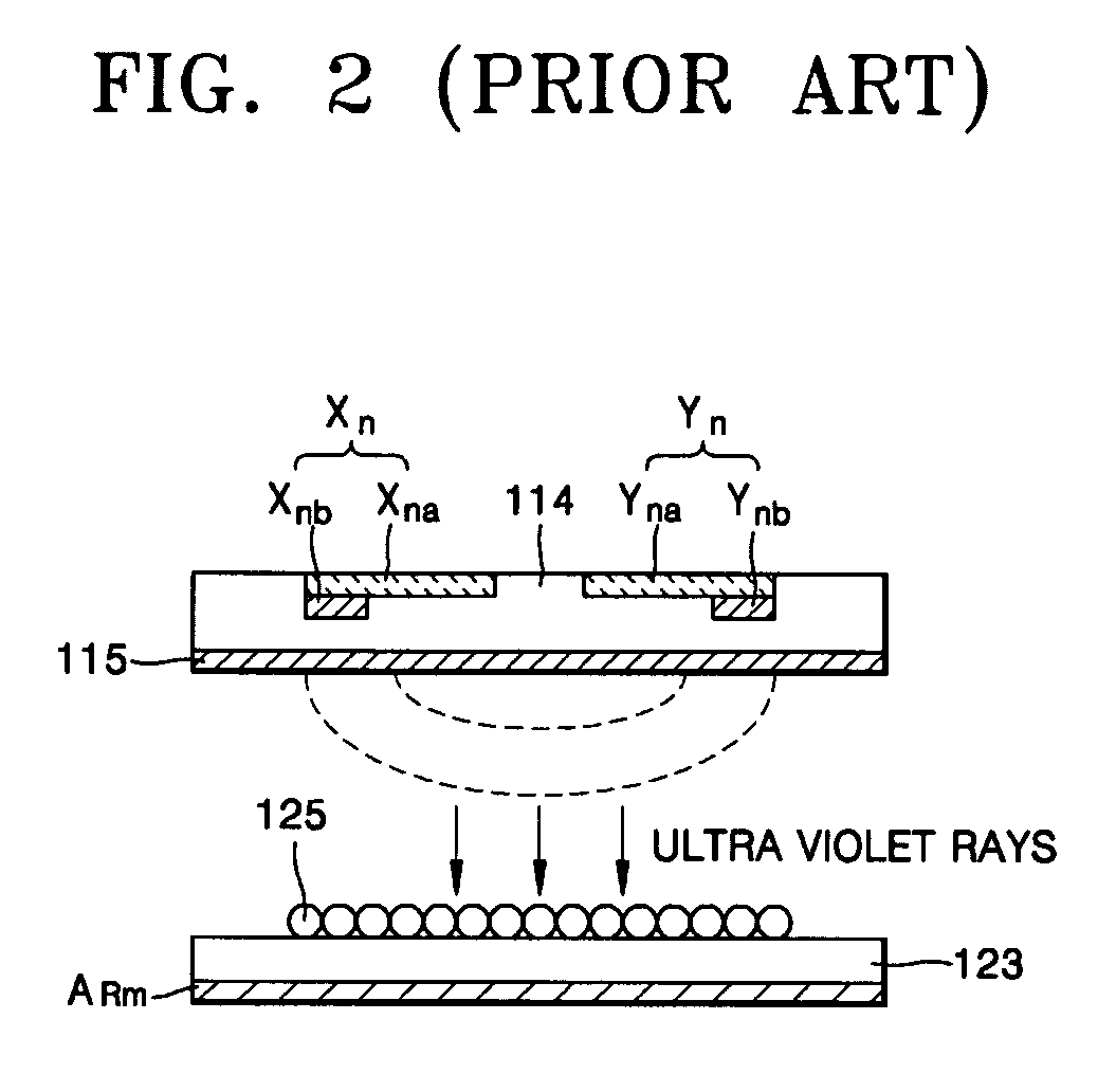
These meta-stable particles ionize neutron particles by colliding with them since the meta-stable particles have a relatively long lifetime, which may decrease the discharge-sustain and discharge firing voltages.
However, this method may require a high address voltage to induce address discharge, thereby reducing driving efficiency.

Method used


Image

  • Plasma display panel having scan electrode closer to address electrode
  • Plasma display panel having scan electrode closer to address electrode
  • Plasma display panel having scan electrode closer to address electrode

Examples


Embodiment Construction

[0036]The present invention will now be described more fully with reference to the accompanying drawings, in which exemplary embodiments of the invention are shown.

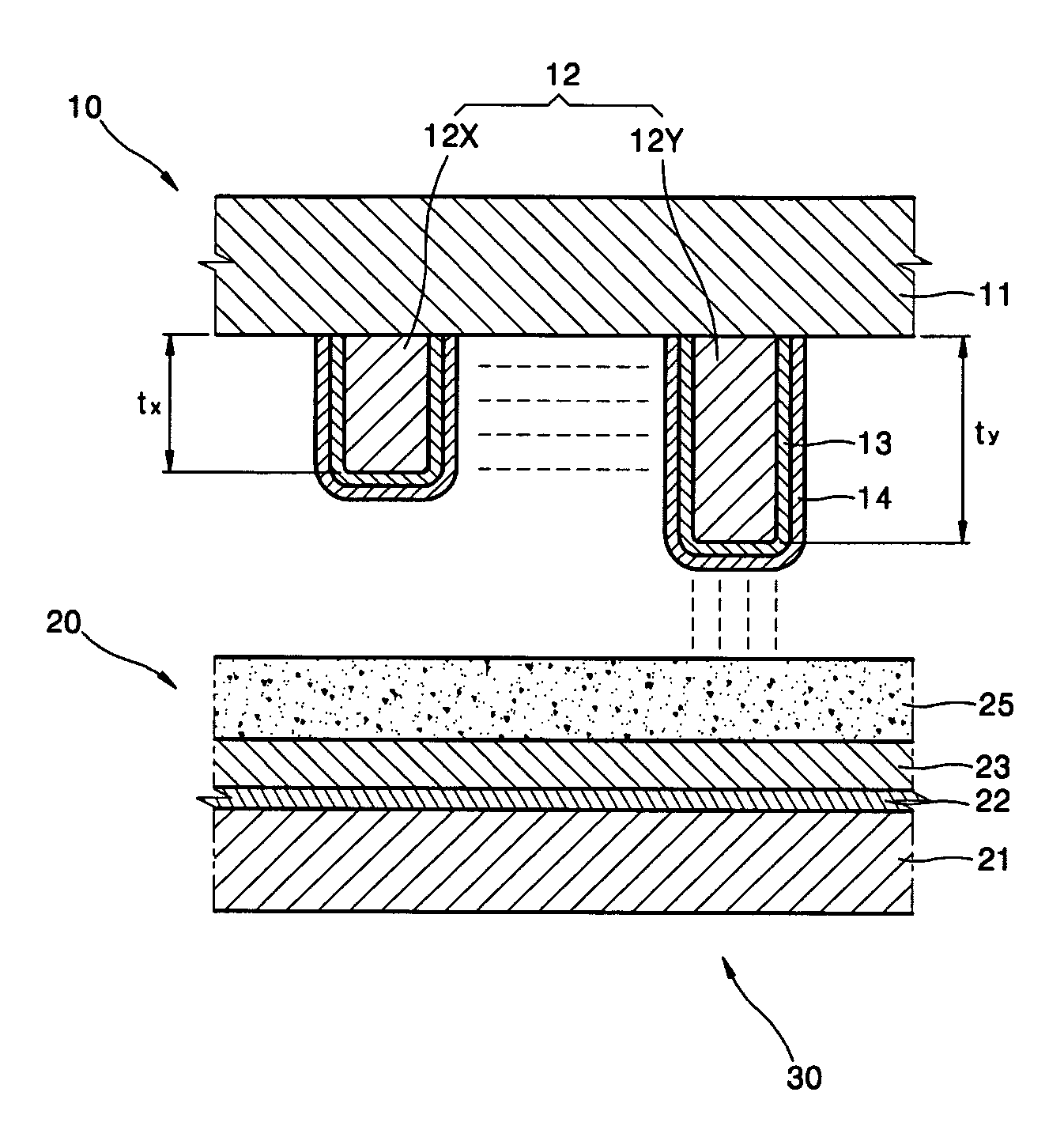
[0037]FIG. 4 is a perspective view showing a PDP according to a first exemplary embodiment of the present invention, and FIG. 5 is a cross-sectional view taken along a line A-A of FIG. 4.

[0038]Referring to FIG. 4 and FIG. 5, a PDP 30 comprises a first panel 10 and a second panel 20 facing each other.

[0039]The first panel 10 comprises a first substrate 11, a discharge sustaining electrode pair 12, a first dielectric layer 13, and a protective layer 14.

[0040]The first substrate 11 may be a glass substrate. A plurality of discharge sustaining electrode pairs 12 may be formed on the first substrate 11 in a stripe pattern, and each discharge sustaining electrode pair comprises a sustain electrode 12X and a scan electrode 12Y facing each other. As shown in FIG. 5, the sustain electrode 12X and the scan electrode 12Y may be form...


PUM


Abstract

A plasma display panel comprising a first panel having a plurality of discharge sustaining electrode pairs, and a second panel having a plurality of address electrodes and facing the first panel. A discharge sustaining electrode pair includes a scan electrode and a sustain electrode having discharge surfaces facing each other, and the scan electrode is closer to the address electrode than the sustain electrode. The plasma display panel requires a reduced address voltage and discharge voltage.

Description

CROSS REFERENCE TO RELATED APPLICATION[0001]This application claims priority to and the benefit of Korean Patent Application No. 10-2003-0086055, filed on Nov. 29, 2003, which is hereby incorporated by reference for all purposes as if fully set forth herein.BACKGROUND OF THE INVENTION[0002]1. Field of the Invention[0003]The present invention relates to a plasma display panel (PDP), and more particularly, to a PDP having improved driving efficiency and brightness.[0004]2. Discussion of the Background[0005]Generally, a PDP displays images by using a discharge effect. It is thin and may have a large screen, as well as high display capacity, high brightness, high contrast, clear latent imagery, and large viewing angle. Therefore, PDPs are considered to be a next generation display device for replacing the cathode ray tube (CRT).[0006]The PDP may be categorized as a direct current (DC) type PDP and an alternating current (AC) type PDP according to its driving voltage waveforms and discha...

Claims


Application Information

Patent Timeline
Patent Type & Authority Patents(United States)
IPC IPC(8): H01J17/49G09G3/28H01J17/04
CPCH01J11/12H01J11/32H01J2211/245H01J2211/323H01J11/24H01J11/26H01J11/38H01J11/40
Inventor KO, JI-SUNG
Owner SAMSUNG SDI CO LTD
Learn More