DC converter

a dc converter and converter technology, applied in bridges, process and machine control, instruments, etc., can solve the problems of destabilizing the operation of dc converters and increasing switching noise, so as to reduce switching loss and noise, increase switching noise, and eliminate delay effects

Inactive Publication Date: 2008-06-03
SANKEN ELECTRIC CO LTD
View PDF5 Cites 16 Cited by
  • Summary
  • Abstract
  • Description
  • Claims
  • Application Information

AI Technical Summary

Benefits of technology

[0018]As shown in FIG. 3, there is a delay between bottom detection at t31 and a turn-on point t32 of the main switch Q1. This delay is the sum of a control delay and a driver delay. In this case, a turn-on point of the main switch Q1 delays behind the point at which the bottom voltage occurs. It is necessary, therefore, to provide a circuit for minimizing the delay between bottom detection and a turn-on point of the main switch Q1. Also, the main switch Q1 must be turned on at high speed. This, however, increases switching noise.
[0019]According to the present invention, a DC converter capable of operating stably without regard to a bottom detection error or a bottom detection variation, eliminating the influence of a delay between a bottom detection point and a turn-on point of a main switch, and reducing a switching loss and noise in all states from a steady state to a transient state, can be provided.

Problems solved by technology

This severely destabilizes the operation of the DC converter.
This, however, increases switching noise.

Method used


Image

  • DC converter
  • DC converter
  • DC converter

Examples


first embodiment

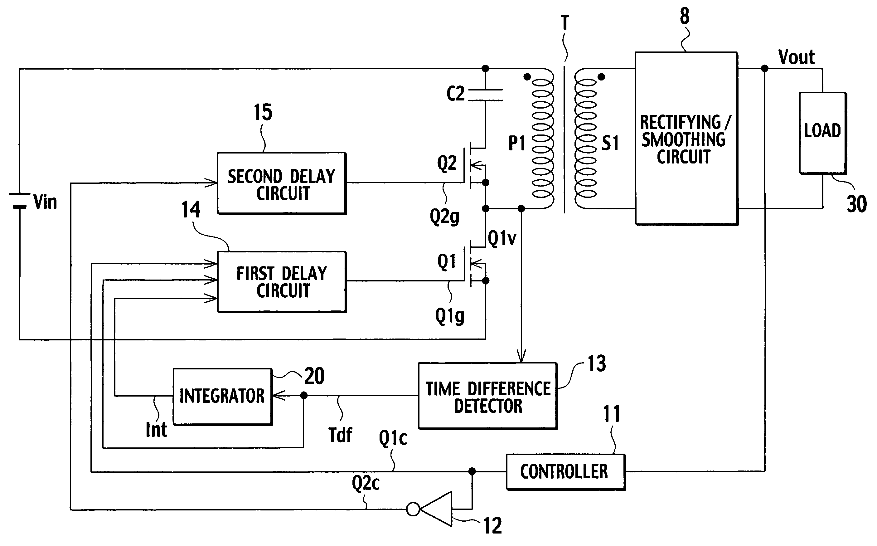
[0061]FIG. 4 is a circuit diagram showing a DC converter according to the first embodiment of the present invention. In FIG. 4, parts corresponding to those of FIG. 1 are represented with the same reference numerals.

[0062]In the DC converter of FIG. 4, a DC power source Vin is connected through a primary winding P1 of a transformer T to a main switch Q1 that is a FET. Ends of the primary winding P1 are connected to a series circuit including an auxiliary switch Q2 that is a FET and a clamp capacitor C2. The main switch Q1 and auxiliary switch Q2 have a dead time in which the switches Q1 and Q2 are OFF. The switches Q1 and Q2 are alternately turned on / off under PWM control carried out by a controller 11.

[0063]The primary winding P1 and a secondary winding S1 of the transformer are wound to generate in-phase voltages. The secondary winding S1 is connected to a rectifying / smoothing circuit 8, so that a voltage (on / off-controlled pulse voltage) induced on the secondary winding S1 is rec...

second embodiment

[0117]FIG. 20 is a circuit diagram showing a DC converter according to the second embodiment of the present invention. This DC converter includes a first time difference detector 13a and a second time difference detector 13b whose minimum voltage detecting sensitivity is lower than that of the first time difference detector 13a.

[0118]The first time difference detector 13a detects a time difference between a point around which a main switch Q1 provides a minimum voltage (bottom level) after an auxiliary switch Q2 turns off and a point when the main switch Q1 turns on, and provides a time difference detection signal Tdfa to an integrator 20. The second time difference detector 13b detects a time difference between a point around which the main switch Q1 provides a minimum voltage after the auxiliary switch Q2 turns off and a point when the main switch Q1 turns on, and provides a time difference detection signal Tdfb as a pulse-by-pulse control signal to a first delay circuit 14.

[0119...

third embodiment

[0131]FIG. 24 is a circuit diagram showing a DC converter according to the third embodiment of the present invention. The DC converter of the third embodiment includes a time difference detector 13 and a voltage change detector 22. Namely, the third embodiment employs the voltage change detector 22 instead of the second time difference detector 13b of FIG. 20.

[0132]The voltage change detector 22 detects a temporal change dV / dt in a voltage Q1v of a main switch Q1 and supplies a pulse-by-pulse control signal representative of the temporal change in the voltage Q1v to a first delay circuit 14. The first delay circuit 14 uses the output of an integrator 20 and the output of the voltage change detector 22 to delay a turn-on point of the main switch Q1. The first delay circuit 14 uses the output of the integrator 20 to minimize the output of the time difference detector 13. Based on the pulse-by-pulse control signal from the voltage change detector 22, the first delay circuit 14 controls...


PUM


Abstract

A DC converter includes a time difference detector to detect a time difference between a point around which a main switch provides a minimum voltage after an auxiliary switch turns off and a point at which the main switch turns on, an integrator to integrate the output of the time difference detector, and a first delay circuit to control a turn-on point of the main switch according to the output of the integrator and the output of the time difference detector. The first delay circuit operates to minimize the output of the time difference detector according to the output of the integrator and controls a turn-on point of the main switch in a pulse-by-pulse manner according to a pulse-by-pulse control signal based on the output of the time difference detector.

Description

BACKGROUND OF THE INVENTION[0001]1. Field of the Invention[0002]The present invention relates to a DC converter with high efficiency and low noise.[0003]2. Description of the Related Art[0004]FIG. 1 shows a DC converter according to a related art. The DC converter of FIG. 1 employs an active clamp method and includes a DC power source Vin, a transformer T having a primary winding P1 (the number of turns is n1) connected to the DC power source Vin, and a main switch Q1 connected to the primary winding P1. The main switch Q1 is a MOSFET (hereinafter referred to as “FET”). Ends of the primary winding P1 are connected to a series circuit consisting of an auxiliary switch Q2 and a clamp capacitor C2. The auxiliary switch Q2 is a FET. The main switch Q1 and auxiliary switch Q2 have a dead time in which both of them are OFF. The switches Q1 and Q2 are alternately turned on / off under PWM control conducted by a controller 111.[0005]The transformer T has the primary winding P1 and a secondary...

Claims


Application Information

Patent Timeline
Patent Type & Authority Patents(United States)
IPC IPC(8): H02M3/335
CPCH02M3/335H02M3/33507H02M1/342Y02B70/10E01D19/086F16L11/14
Inventor ASO, SHINJIFURUKOSHI, RYUICHIOHTAKE, OSAMU
Owner SANKEN ELECTRIC CO LTD
Why Eureka
Try Eureka