Laser treatment apparatus, laser treatment method, and manufacturing method of semiconductor device

Inactive Publication Date: 2008-07-01
SEMICON ENERGY LAB CO LTD
View PDF6 Cites 4 Cited by
  • Summary
  • Abstract
  • Description
  • Claims
  • Application Information

AI Technical Summary

Benefits of technology

[0014]It is an object of the present invention to provide a laser treatment apparatus and a laser treatment method which do not cause a disaster such as a fire even when an abnormal stop, a malfunction, or the like occurs.
[0030]According to the invention, laser output can be automatically stopped when a stage of a laser treatment apparatus is abnormally stopped or the apparatus is vibrated by an earthquake or the like. Thus, a disaster such as a fire can be prevented. Further, a similar effect can be obtained also when a PC which controls stage movement or laser output is frozen (abnormally stopped).

Problems solved by technology

Meanwhile, an injury, a fire, and the like are major disasters which occur in performing laser annealing.
A disaster such as a fire in performing laser annealing is thought to be caused by an abnormal stop of a stage which moves a substrate (for example, an XY stage), vibration of an apparatus due to an earthquake or the like, generation of an abnormal gas, generation of smoke, a change in an optical system such as a mirror due to high heat, or the like.
When a stage is abnormally stopped at an unexpected position during laser annealing, a portion below an intended irradiation position may ignite, or a portion therearound may ignite due to reflected light from an unspecified position or the like, which is very dangerous.

Method used


Image

  • Laser treatment apparatus, laser treatment method, and manufacturing method of semiconductor device
  • Laser treatment apparatus, laser treatment method, and manufacturing method of semiconductor device
  • Laser treatment apparatus, laser treatment method, and manufacturing method of semiconductor device

Examples


embodiment 1

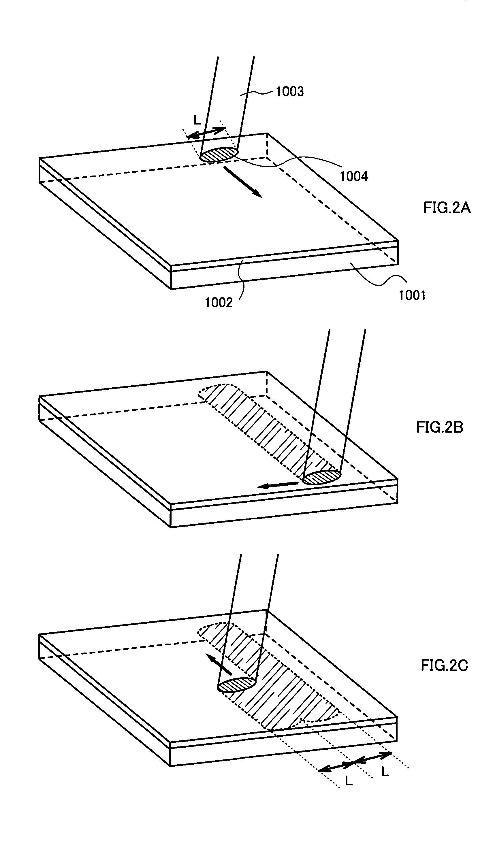
[0078]In this embodiment, a method for manufacturing a semiconductor device using the laser treatment apparatus of the invention is explained with reference to FIGS. 4A to 4D, 5A to 5C, and 6A to 6C.

[0079]First, as shown in FIG. 4A, a base film 501 is formed over a substrate 500. As the substrate 500, a glass substrate of, for example, barium borosilicate glass, aluminoborosilicate glass, or the like, a quartz substrate, a stainless-steel substrate, or the like can be used. A substrate made of a synthetic resin having flexibility such as acrylic or plastic typified by PET, PES, or PEN can alternatively be used.

[0080]The base film 501 is provided to prevent alkali metal such as Na and alkaline earth metal contained in the substrate 500 from diffusing into a semiconductor film and adversely affecting characteristics of a semiconductor element. Therefore, the base film 501 is formed using an insulating film of silicon oxide (SiO), silicon nitride (SiN), silicon oxide containing nitroge...

embodiment 2

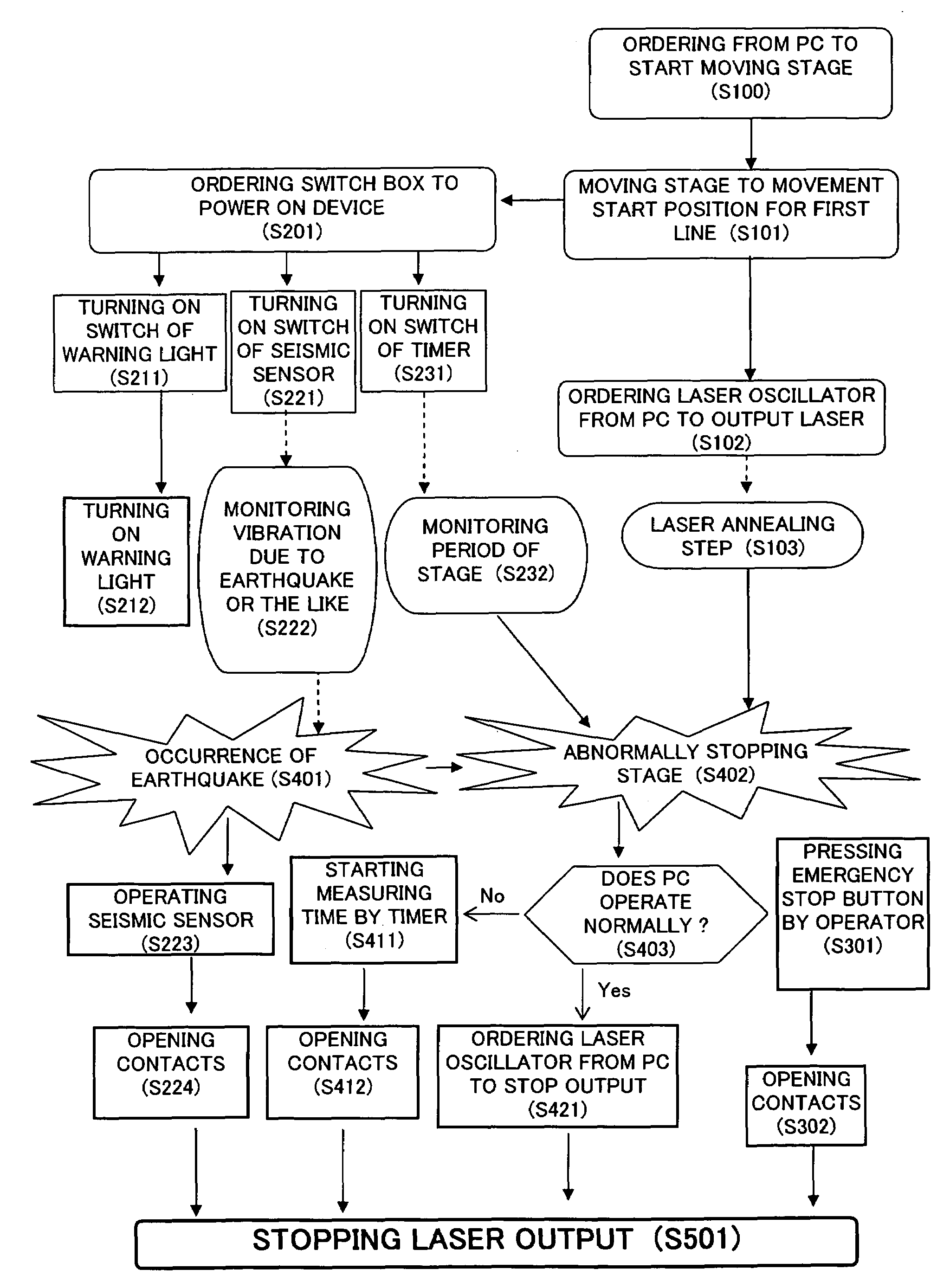
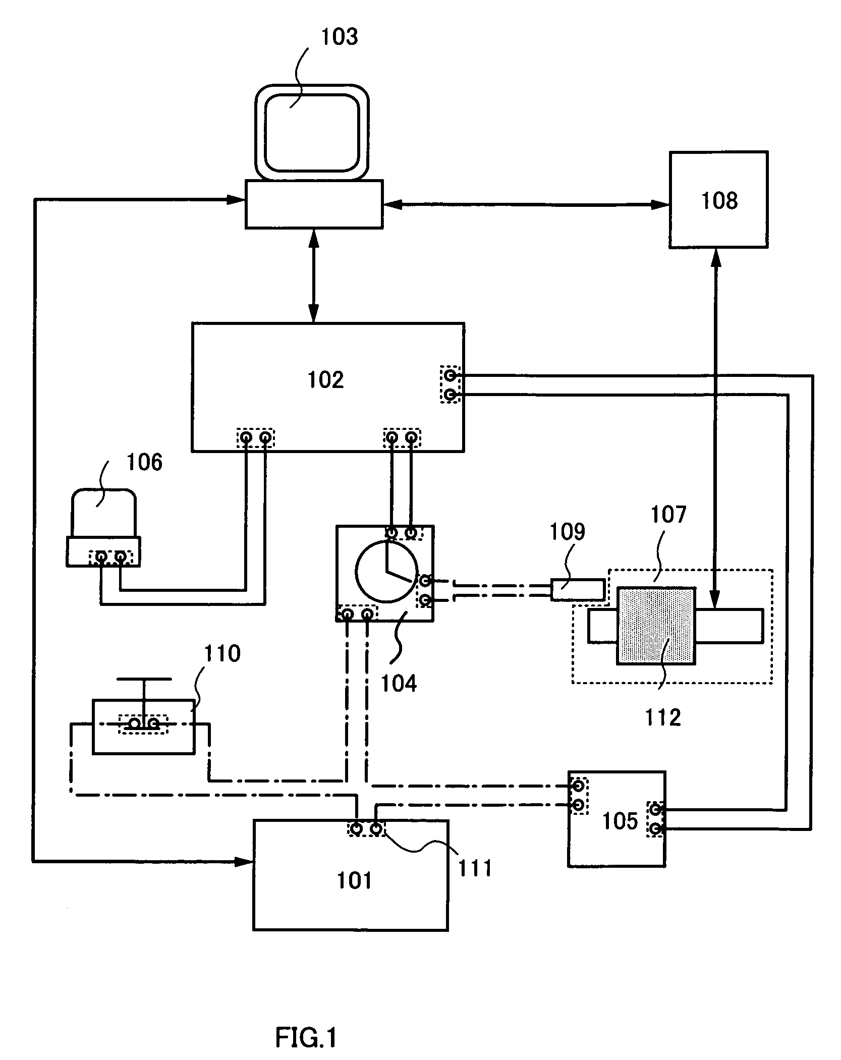
[0148]In this embodiment, a method for stopping laser irradiation, which is different from that described in Embodiment 1, is explained with reference to FIG. 7A to FIG. 7B.

[0149]If a movable table 303 operates normally, a substrate over the movable table 303 is irradiated with a linear laser which is outputted from a laser oscillator 301.

[0150]If the movable table 303 is in an abnormal situation, conduction between contacts of a timer is blocked as in Embodiment 1. This embodiment differs from Embodiment 1 in that an electromagnetic shutter 302 connected to the timer is provided between the laser oscillator 301 and the movable table 303, and at the time of abnormal movement of the movable table 303, the electromagnetic shutter 302 interrupts an optical path of the linear laser so as not to irradiate a portion other than the movable table 303 with the linear laser (FIG. 7A).

[0151]The electromagnetic shutter 302 includes an air cylinder 304 and a solenoid valve 305. An end of the air...


PUM

PropertyMeasurementUnit
frequencyaaaaaaaaaa
frequencyaaaaaaaaaa
longitudinal lengthaaaaaaaaaa

Abstract

The invention relates to a laser treatment apparatus including a laser oscillator, an interlock provided in the laser oscillator, a movable table which moves with a certain movement period, a timer, an interlock provided in the timer, a sensor which can detect movement of the movable table, and a computer, in which the timer starts measuring time when the sensor senses passage of the movable table, and when the movable table does not pass the sensor even after the movement period, conduction between contacts of the interlock provided in the timer is blocked to operate the interlock in the laser oscillator, thereby stopping laser output. The invention also relates to a laser treatment method using the laser treatment apparatus.

Description

BACKGROUND OF THE INVENTION[0001]1. Field of the Invention[0002]The present invention relates to a laser light irradiation method and a laser treatment apparatus for laser light irradiation. The invention also relates to a method for manufacturing a semiconductor device using laser light irradiation.[0003]2. Description of the Related Art[0004]A laser treatment apparatus which performs various kinds of processing by laser light irradiation and a laser light irradiation method have been known.[0005]One feature of using laser light is that only a region which is irradiated with laser light and absorbs energy thereof can be selectively heated unlike in the case of heat treatment using radiation heating or conduction heating. For example, laser treatment using an excimer laser oscillator, which oscillates ultraviolet light having a wavelength of 400 nm or less, heats a semiconductor film selectively and locally, and achieves crystallization or activation of the semiconductor film with l...

Claims


Application Information

Patent Timeline
Patent Type & Authority Patents(United States)
IPC IPC(8): H01L21/20
CPCB23K26/0853H01L27/1285H01L21/2026B23K2201/40B23K2101/40H01L21/02425H01L21/02686H01L21/02683H01L21/02678H01L21/02422H01L21/02488H01L21/02532H01L21/0242H01L21/02672H01L21/02691
Inventor TANAKA, KOICHIROYAMAMOTO, YOSHIAKIOMATA, TAKATSUGU
Owner SEMICON ENERGY LAB CO LTD
Why Eureka
Try Eureka