Spin-injection magnetic random access memory

a magnetic random access and magnetic technology, applied in information storage, static storage, digital storage, etc., can solve the problems of increasing power consumption at a write time, memory capacity cannot be enlarged, and the cell size cannot be reduced to be less than that of a dynamic random access memory (dram)

Active Publication Date: 2008-07-01
KK TOSHIBA
View PDF11 Cites 39 Cited by
  • Summary
  • Abstract
  • Description
  • Claims
  • Application Information

AI Technical Summary

Problems solved by technology

However, in a case where an architecture is adopted in which a memory cell is constituted of one transistor and one magnetoresistive element, there is a problem that a cell size cannot be reduced to be not more than that of a dynamic random access memory (DRAM).
This causes new problems that power consumption at a write time increases, a memory capacity cannot be enlarged owing to a limit of a tolerable current density of a wiring line, and an area of a driver / sinker which generates the current pulse enlarges.
However, the value of the write current cannot be reduced to 1 mA or less.

Method used


Image

  • Spin-injection magnetic random access memory
  • Spin-injection magnetic random access memory
  • Spin-injection magnetic random access memory

Examples


embodiment

2. EMBODIMENT

[0058]Next, there will be described several embodiments supposed to be the best.

first embodiment

(1) First Embodiment

[0059]A first embodiment is an example in which a path of a spin-injection current is completely separated from that of an assist current.

[0060]A. Circuit Diagram

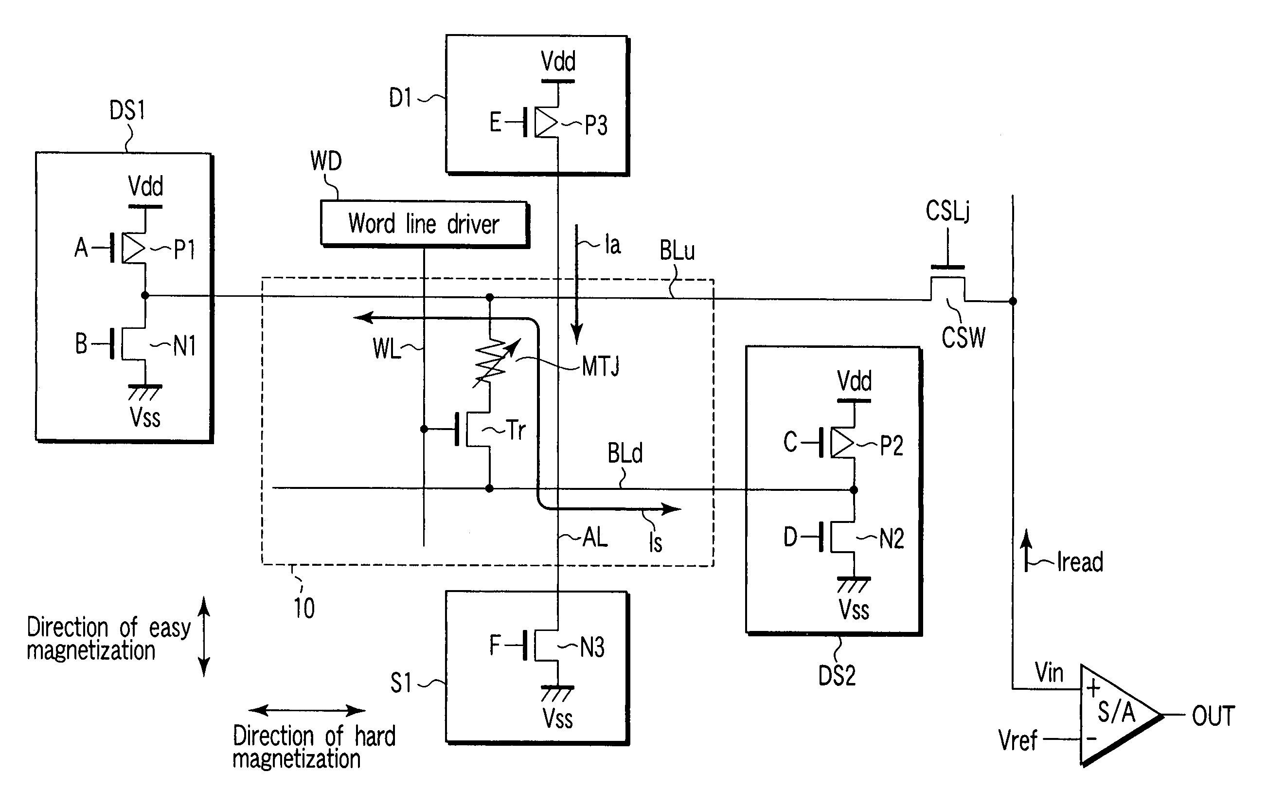
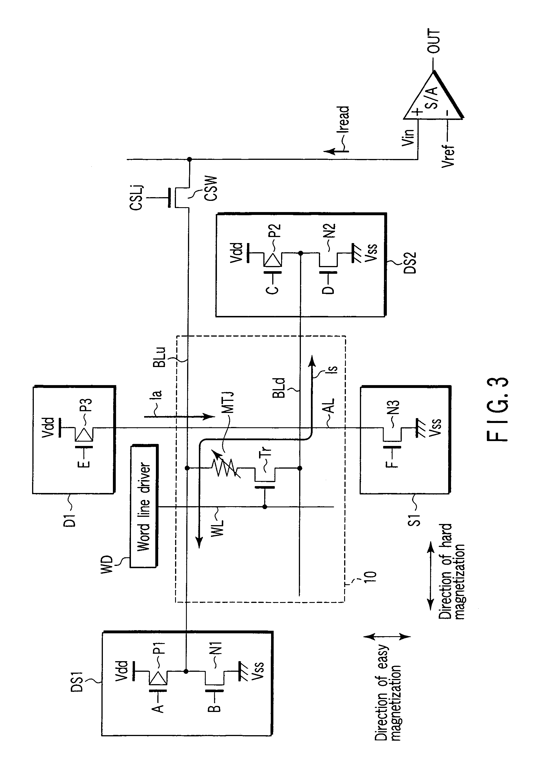
[0061]FIG. 3 is a circuit diagram showing a main part of a magnetic random access memory in a first embodiment.

[0062]A magnetoresistive element MTJ constitutes a part of a memory cell array 10.

[0063]One end of the magnetoresistive element MTJ is connected to an upper bit line BLu, and the other end thereof is connected to a lower bit line BLd via an N-channel MOS transistor Tr as a selection switch. Both of the upper bit line BLu and the lower bit line BLd extend in the same direction which is a direction of a hard magnetization (column direction) of the magnetoresistive element MTJ in the present example.

[0064]One end of the upper bit line BLu is connected to a CMOS type driver / sinker DS1. The driver / sinker DS1 is constituted of a P-channel MOS transistor P1 and an N-channel MOS transistor N1 connected ...

second embodiment

(2) Second Embodiment

[0106]A second embodiment is an example in which a path of a spin-injection current partially agrees with that of an assist current.

[0107]A. Circuit Diagram

[0108]FIG. 6 is a circuit diagram showing a first example of a main part of a magnetic random access memory in a second embodiment.

[0109]A magnetoresistive element MTJ constitutes a part of a memory cell array 10.

[0110]One end of the magnetoresistive element MTJ is connected to an upper bit line BLu / write assist line AL, and the other end thereof is connected to a lower bit line BLd via an N-channel MOS transistor Tr as a selection switch.

[0111]Both of the upper bit line BLu / write assist line AL and the lower bit line BLd extend in the same direction which is a direction of an easy magnetization (column direction) of the magnetoresistive element MTJ in the present example.

[0112]One end of the upper bit line BLu / write assist line AL is connected to CMOS type drivers / sinkers DS1 and DS3.

[0113]The driver / sinker ...


PUM


Abstract

A spin-injection magnetic random access memory of an aspect of the present invention includes a magnetoresistive element, a unit which writes data into the magnetoresistive element by use of spin-polarized electrons generated by a spin-injection current and which applies, to the magnetoresistive element, a magnetic field of a direction of a hard magnetization of the magnetoresistive element during the writing.

Description

CROSS-REFERENCE TO RELATED APPLICATIONS[0001]This application is based upon and claims the benefit of priority from prior Japanese Patent Application No. 2005-315459, filed Oct. 28, 2005, the entire contents of which are incorporated herein by reference.BACKGROUND OF THE INVENTION[0002]1. Field of the Invention[0003]The present invention relates to a spin-injection magnetic random access memory which performs magnetization reversal by use of spin-polarized electrons.[0004]2. Description of the Related Art[0005]In recent years, intensive attempts have been made to apply a magnetoresistive element utilizing a tunneling magneto resistance (TMR) effect to a magnetic random access memory (MRAM).[0006]In recent years, a magnetoresistive element has been obtained whose magnetoresistive (MR) ratio indicating a magnetoresistive change ratio is 230% or more, and dependence of the MR ratio on a voltage has been suppressed. This increases a possibility of putting the magnetic random access memo...

Claims


Application Information

Patent Timeline
Patent Type & Authority Patents(United States)
IPC IPC(8): G11C11/00
CPCG11C11/16
Inventor INOKUCHI, TOMOAKISAITO, YOSHIAKISUGIYAMA, HIDEYUKI
Owner KK TOSHIBA
Why Eureka
Try Eureka