Bipolar transistor

a bipolar transistor and transistor technology, applied in the field of integrated circuit technology, can solve problems such as giving a slower transport, and achieve the effect of eliminating the effect of base push out effects

Inactive Publication Date: 2008-07-08
INFINEON TECH AG
View PDF9 Cites 2 Cited by
  • Summary
  • Abstract
  • Description
  • Claims
  • Application Information

AI Technical Summary

Benefits of technology

[0008]It is an object of the present invention to provide a monolithically integrated bipolar transistor on an SOI (Silicon-On-Insulator) substrate, wherein base push out effects are eliminated, or at least severely reduced.
[0013]According to a first aspect of the present invention, there is provided a monolithically integrated bipolar transistor having an SOI (Silicon-On-Insulator) substrate, a collector region in the SOI substrate, a base layer region on top of and in contact with the collector region, and an emitter layer region on top of and in contact with the base layer region, wherein the collector, base layer, and emitter layer regions are provided with separate contact regions. Further, a region of an insulating material is provided in the base layer region, in the emitter layer region, or between the base and emitter layer regions, wherein the region of the insulating material extends laterally at a fraction of a width of the base and emitter layer regions to reduce an effective width of the bipolar transistor.

Problems solved by technology

However the oxide interface prevents all transport and the entire collector layer becomes flooded with carriers, giving a slower transport.

Method used


Image

  • Bipolar transistor
  • Bipolar transistor
  • Bipolar transistor

Examples


Embodiment Construction

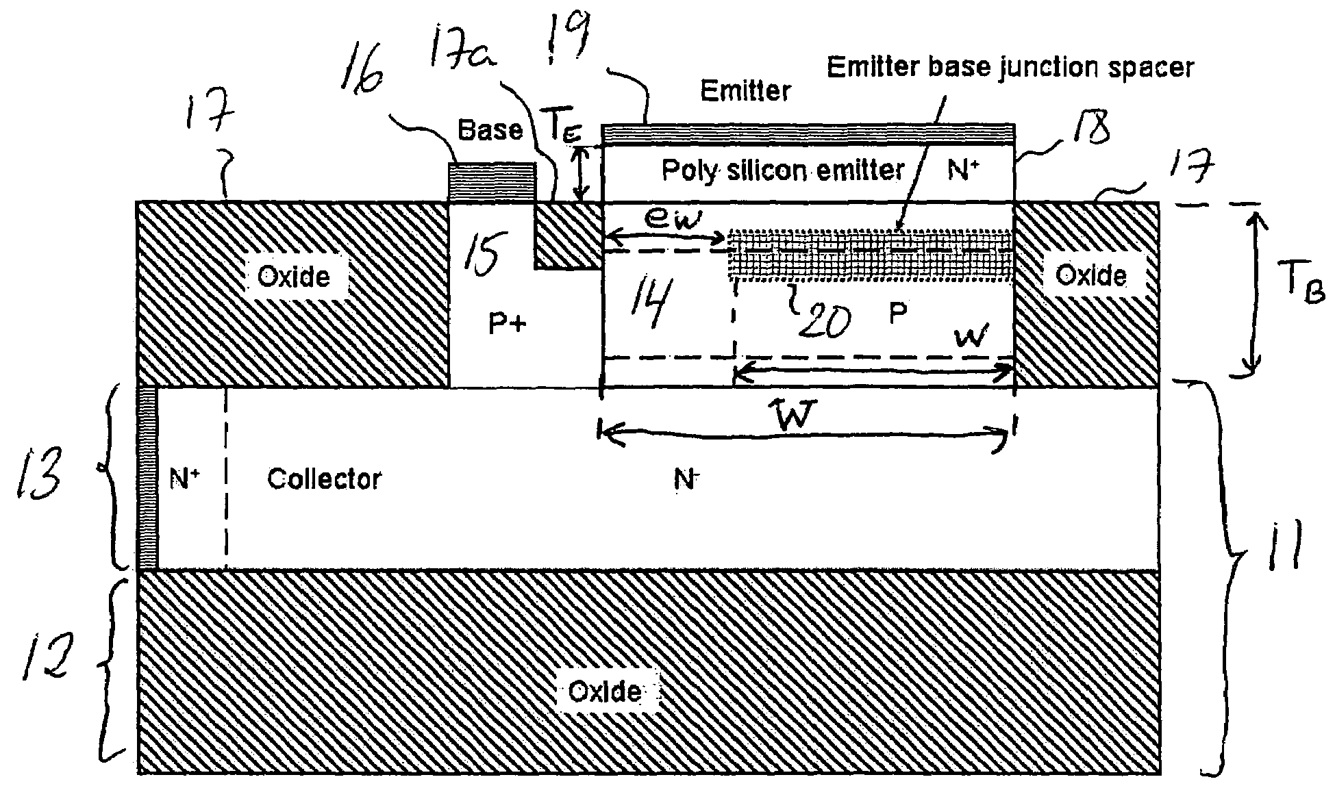
[0022]A partially processed monolithically integrated bipolar transistor according to a preferred embodiment of the present invention is shown in FIG. 1 in cross section. A common SOI structure substrate 11 comprises a buried silicon oxide layer 12 and a monocrystalline silicon layer thereupon. The monocrystalline silicon layer is a thin layer and may have a thickness of less than about 200 nm.

[0023]The inventive bipolar transistor comprises a lateral collector region 13 doped to N− and N+ in the monocrystalline silicon layer of the SOI structure substrate 11, an essentially planar P-type doped intrinsic base layer region 14 thereon, and finally an essentially planar N+-type doped emitter layer region 18 thereon. The collector 13, base layer 14, and emitter layer 18 regions are provided with separate contact regions.

[0024]The collector comprises an N+-type doped collector contact region, which contacts the collector to e.g. the upper surface of the structure (not illustrated). The P...


PUM


Abstract

A monolithically integrated bipolar transistor has an SOI substrate, a collector region in the SOI substrate, a base layer region on top of and in contact with the collector region, and an emitter layer region on top of and in contact with the base layer region, wherein the collector, base layer, and emitter layer regions are provided with separate contact regions. Further, a region of an insulating material, preferably an oxide or nitride, is provided in the base layer region, in the emitter layer region, or between the base and emitter layer regions, wherein the insulating region extends laterally at a fraction of a width of the base and emitter layer regions to reduce an effective width of the bipolar transistor to thereby eliminate any base push out effects that would otherwise occur.

Description

CROSS-REFERENCE TO RELATED APPLICATION[0001]This application claims priority from European Patent Application No. 04005895.0, filed on Mar. 12, 2004, and is incorporated herein by reference in its entirety.BACKGROUND OF THE INVENTION[0002]1. Field of the Invention[0003]The present invention generally relates to the field of integrated circuit technology, and more specifically the invention relates to a monolithically integrated bipolar transistor on an SOI (Silicon-On-Insulator) substrate.[0004]2. Description of Related Art[0005]Bipolar transistors in SOI technologies using thin silicon layers are often designed by means of a vertical emitter-base structure and a lateral collector structure, see e.g. U.S. Pat. No. 5,087,580 to Eklund, and J. Cai et al., Vertical SiGe-Base Bipolar Transistors on CMOS-Compatible SOI Substrate, p. 215 in Proceedings of the 2003 Bipolar / BiCMOS Circuits and Technology Meeting.[0006]Depending on the geometry, this design may be limited by base push out ef...

Claims


Application Information

Patent Timeline
Patent Type & Authority Patents(United States)
IPC IPC(8): H01L27/082H01L21/331H01L29/73H01L29/732H01L29/76
CPCH01L29/7317
Inventor ARNBORG, TORKEL
Owner INFINEON TECH AG
Why Eureka
Try Eureka