Laser annealing apparatus and annealing method of semiconductor thin film using the same

a laser annealing and semiconductor thin film technology, applied in the direction of optical radiation measurement, instruments, manufacturing tools, etc., can solve the problems of reducing the life of the xy stage, increasing the size and weight of the substrate, and so as to reduce the throughput and prolong the stage life , the effect of reducing the cost of the apparatus

Inactive Publication Date: 2008-07-08
PANASONIC LIQUID CRYSTAL DISPLAY CO LTD +1
View PDF51 Cites 12 Cited by
  • Summary
  • Abstract
  • Description
  • Claims
  • Application Information

AI Technical Summary

Benefits of technology

[0012]However, with increase in size of substrates, substrates 1 m or more square are to be used. To this end, the rotary stage to be mounted with a substrate also increases in size and weight, resulting in a large load in scanning with a laser beam in each of the X- and Y-directions. Particularly in high-speed scanning or in high-accuracy scanning, the heavy rotary stage must be moved together. Thus, not only is it necessary to increase the size of the XY stage, enhance the rigidity of the XY stage, and further take measures to suppress vibrations of the apparatus as a whole, but the life of the XY stage may be also shortened due to the large load. As a result, there is a problem that the manufacturing cost and the operation cost of the apparatus are increased.
[0014]To solve the foregoing problems belonging to the background art, it is an object of the present invention to provide a laser annealing method and a laser annealing apparatus in which a stage is reduced in size and weight and extended in life, and the apparatus cost is reduced, so that the method and the apparatus are suitable for manufacturing a display panel.
[0027]As described above, according to the laser annealing apparatus and the laser annealing method according to the present invention, annealing by scanning a substrate with a laser beam in two directions crossing each other at right angles can be performed only by changing the moving direction of the substrate without rotating the substrate. That is, as a stage for high-speed or high-accuracy scanning of a substrate mounted thereon, it will go well if the stage is driven in the X- and Y-directions. It is not necessary to place a rotary stage on an XY stage. Accordingly, a load on the XY stage can be reduced so that the life of the stage can be extended, and hence the apparatus cost can be reduced. If the substrate is rotated, it will be necessary to perform realignment so that the throughput will be lowered. However, when the optical axis of the laser beam is rotated, it is not necessary to perform realignment. Thus, the present invention is effective also in terms of improvement in throughput.

Problems solved by technology

To this end, the rotary stage to be mounted with a substrate also increases in size and weight, resulting in a large load in scanning with a laser beam in each of the X- and Y-directions.
Thus, not only is it necessary to increase the size of the XY stage, enhance the rigidity of the XY stage, and further take measures to suppress vibrations of the apparatus as a whole, but the life of the XY stage may be also shortened due to the large load.
As a result, there is a problem that the manufacturing cost and the operation cost of the apparatus are increased.
It is necessary to rotate the shaped beam without rotating the homogenizer constituted by the cylindrical lens array which is a complicated optical system.

Method used


Image

  • Laser annealing apparatus and annealing method of semiconductor thin film using the same
  • Laser annealing apparatus and annealing method of semiconductor thin film using the same
  • Laser annealing apparatus and annealing method of semiconductor thin film using the same

Examples


embodiment 1

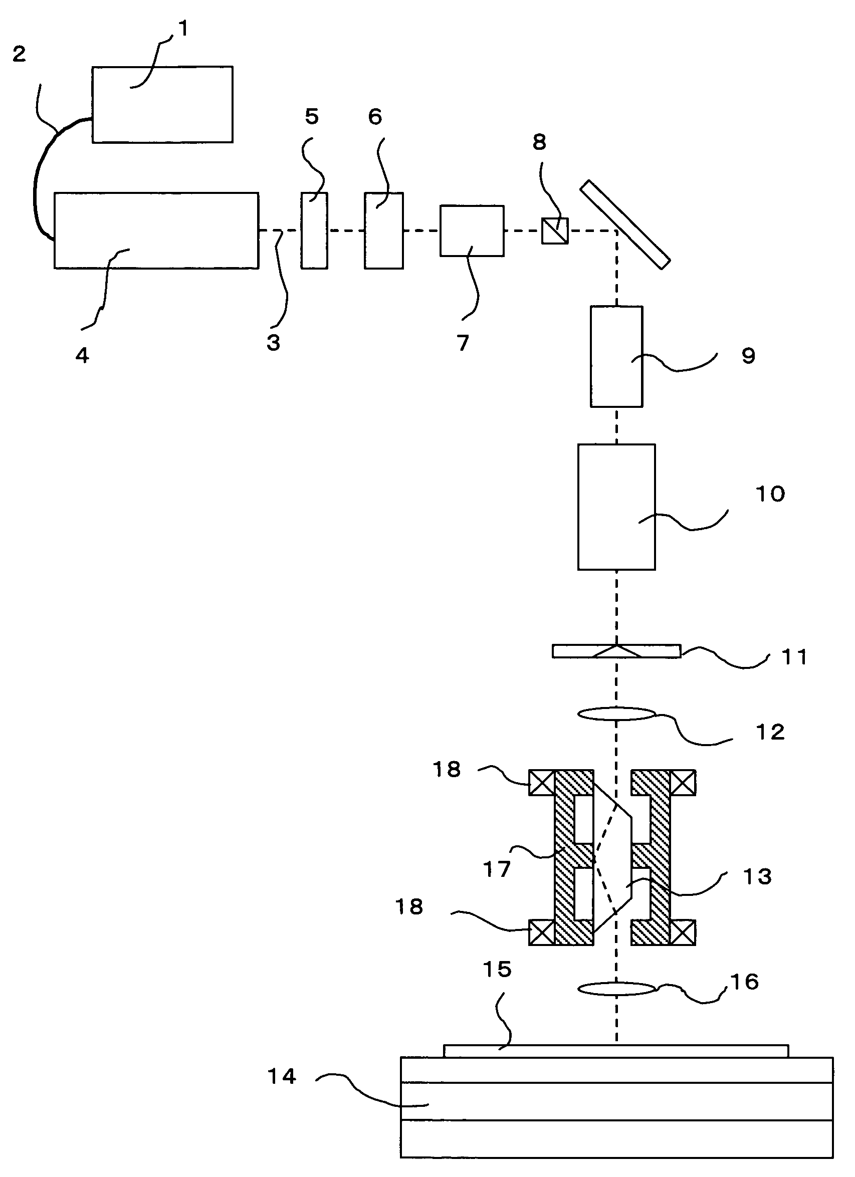
[0040]An embodiment of the present invention will be described below in detail with reference to the drawings. FIG. 1 is a view showing the configuration of an optical system of a laser annealing apparatus according to Embodiment 1 of the present invention. In FIG. 1, the laser annealing apparatus is constituted by a laser oscillator 4 coupled with a pumping LD (Laser Diode) 1 though a fiber 2 and for generating a continuous wave laser beam 3, a shutter 5 for turning on / off the laser beam 3, a continuously variable transmittance ND filter 6 for adjusting the energy of the laser beam 3, an electro-optic modulator (hereinafter referred to as “EO modulator”) 7 for pulsing the laser beam 3 output from the laser oscillator 4 and temporally amplitude modulating the energy of the laser beam 3, a polarized beam splitter 8, a beam expander (or beam reducer) 9 for adjusting the beam diameter of the laser beam 3, a beam shaper (beam homogenizer) 10 for shaping the laser beam 3 into a long and ...

embodiment 2

[0061]Next, description will be made about Embodiment 2 according to the present invention. FIG. 6 is a view showing the configuration of an optical system of a laser annealing apparatus according to Embodiment 2 of the present invention. Incidentally, parts the same as those in FIG. 1 are denoted by the same reference numerals correspondingly. In FIG. 6, the laser annealing apparatus is constituted by a laser oscillator 4 coupled with a pumping LD (Laser Diode) 1 though a fiber 2 and for generating a continuously wave laser beam 3, a shutter 5 for turning on / off the laser beam 3, a continuously variable transmittance ND filter 6 for adjusting the energy of the laser beam 3, an electro-optic modulator (hereinafter referred to as “EO modulator”) 7 for pulsing the laser beam 3 output from the laser oscillator 4 and temporally amplitude modulating the energy of the laser beam 3, a polarized beam splitter 8, a beam expander (or beam reducer) 9 for adjusting the beam diameter of the lase...

embodiment 3

[0074]Next, an embodiment of a laser annealing method according to the present invention to be carried out using the aforementioned laser annealing apparatus will be described as Embodiment 3 of the invention. The description will be made with reference to FIG. 1 and FIGS. 7A-7C. FIGS. 7A-7C are views for explaining the embodiment of the laser annealing method according to the present invention. Here, a polycrystalline silicon thin film substrate is used as the substrate 15 (FIG. 1). The polycrystalline silicon thin film substrate is obtained as follows. That is, an amorphous silicon thin film is formed on one principal surface of a glass substrate 101 through an insulator thin film (not shown). The whole surface of the amorphous silicon thin film is scanned with an excimer laser beam so as to be crystallized as a polycrystalline silicon thin film 102. Here, the insulator thin film is an SiO2 film, an SiN film, or a composite film of those. The polycrystalline silicon thin film subs...


PUM

PropertyMeasurementUnit
angleaaaaaaaaaa
sizeaaaaaaaaaa
angleaaaaaaaaaa

Abstract

A laser beam temporally modulated in amplitude by a modulator and shaped into a long and narrow shape by a beam shaper is rotated around the optical axis of an image rotator inserted between the beam shaper and a substrate. Thus, the longitudinal direction of the laser beam having the long and narrow shape is rotated around the optical axis on the substrate. In order to perform annealing in a plurality of directions on the substrate, the laser beam shaped into the long and narrow shape is rotated on the substrate while a stage mounted with the substrate is moved only in two directions, that is, X- and Y-directions.In such a manner, the substrate can be scanned at a high speed with a continuous wave laser beam modulated temporally in amplitude and shaped into a long and narrow shape, without rotating the substrate. Thus, a semiconductor film can be annealed.

Description

BACKGROUND OF THE INVENTION[0001]The present invention relates to a laser annealing method and a laser annealing apparatus suitable for irradiating an amorphous or polycrystalline semiconductor film formed on an insulating substrate with a laser beam so as to improve the film quality or enlarge or mono-crystallize crystal grains.[0002]At present, a flat panel type display unit using a display panel such as a liquid crystal panel or an organic EL panel is developed and put or being put into practical use. The display panel in such a display unit has a large number of pixels in its display region. The pixels are arrayed two-dimensionally (in a matrix) out of thin film transistors (TFTs) formed of an amorphous silicon film or a polycrystalline silicon film formed on a substrate of glass, fused quartz or the like. An image is formed by switching on / off the thin film transistors corresponding to the pixels. The thin film transistors of the pixels are driven and switched by a driver circu...

Claims


Application Information

Patent Timeline
Patent Type & Authority Patents(United States)
IPC IPC(8): H01S3/00H01L21/20B23K26/073G02B27/09G02F1/13H01L21/268H01L21/77
CPCB23K26/0738B23K26/0853G02B27/0927G02B27/0966H01L27/1296H01L21/2026H01L27/1285H01L21/02595H01L21/02686H01L21/02683H01L21/02691H01L21/02422H01L21/02532H01L21/02678G02F1/13
Inventor HONGO, MIKIOYAZAKI, AKIOHATANO, MUTSUKO
Owner PANASONIC LIQUID CRYSTAL DISPLAY CO LTD
Why Eureka
Try Eureka