Apparatus and method for packaging and integrating microphotonic devices

a micro-photonic device and packaging technology, applied in the field of photonics and optoelectronic devices, can solve the problems of suitable use and optical coupling mechanism, and achieve the effect of low loss coupling and maximum coupling of laser ligh

Inactive Publication Date: 2008-07-08
UNITED STATES OF AMERICA AS REPRESENTED BY THE ADMINISTATOR OFNAT AERONAUTICS & SPACE ADMINISTATION THE
View PDF9 Cites 0 Cited by
  • Summary
  • Abstract
  • Description
  • Claims
  • Application Information

AI Technical Summary

Benefits of technology

[0007]It is a further object of the present invention to provide for an optical coupling arrangement that enables low-loss coupling of laser light into and out of a microphotonic resonator disk.
[0008]It is a further object of the present invention to provide for an apparatus that includes means for tuning and adjusting prisms so as to achieve maximum coupling of laser light to and from the microphotonic resonator disk.

Problems solved by technology

Since the optical coupling mechanisms are implemented with bulky components, these optical coupling mechanisms are not suitable for use in integrating and interconnecting all of the microphotonic components and optical devices embodied in, for example, microphotonic millimeter-wave receivers.

Method used


Image

  • Apparatus and method for packaging and integrating microphotonic devices
  • Apparatus and method for packaging and integrating microphotonic devices
  • Apparatus and method for packaging and integrating microphotonic devices

Examples


Embodiment Construction

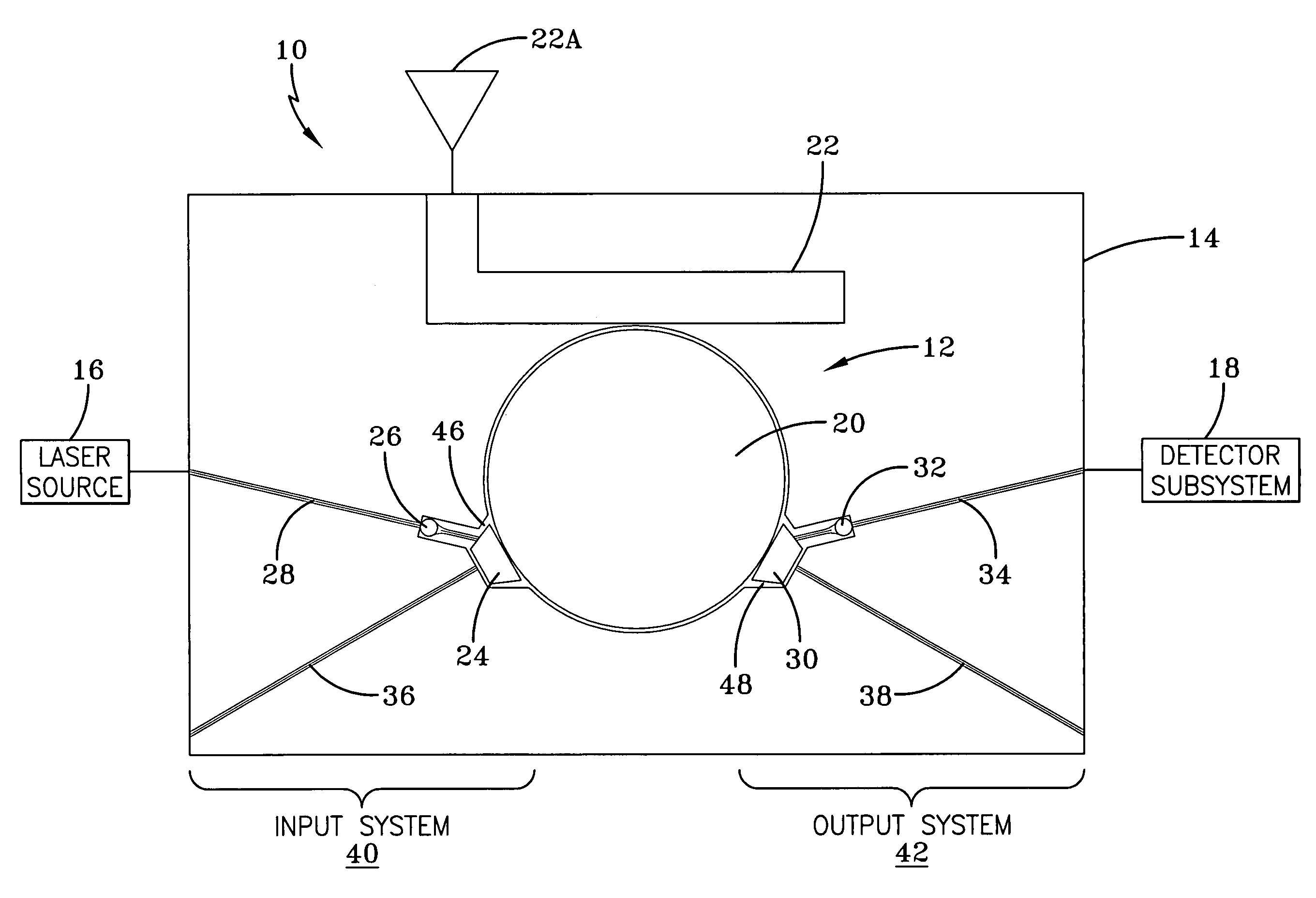
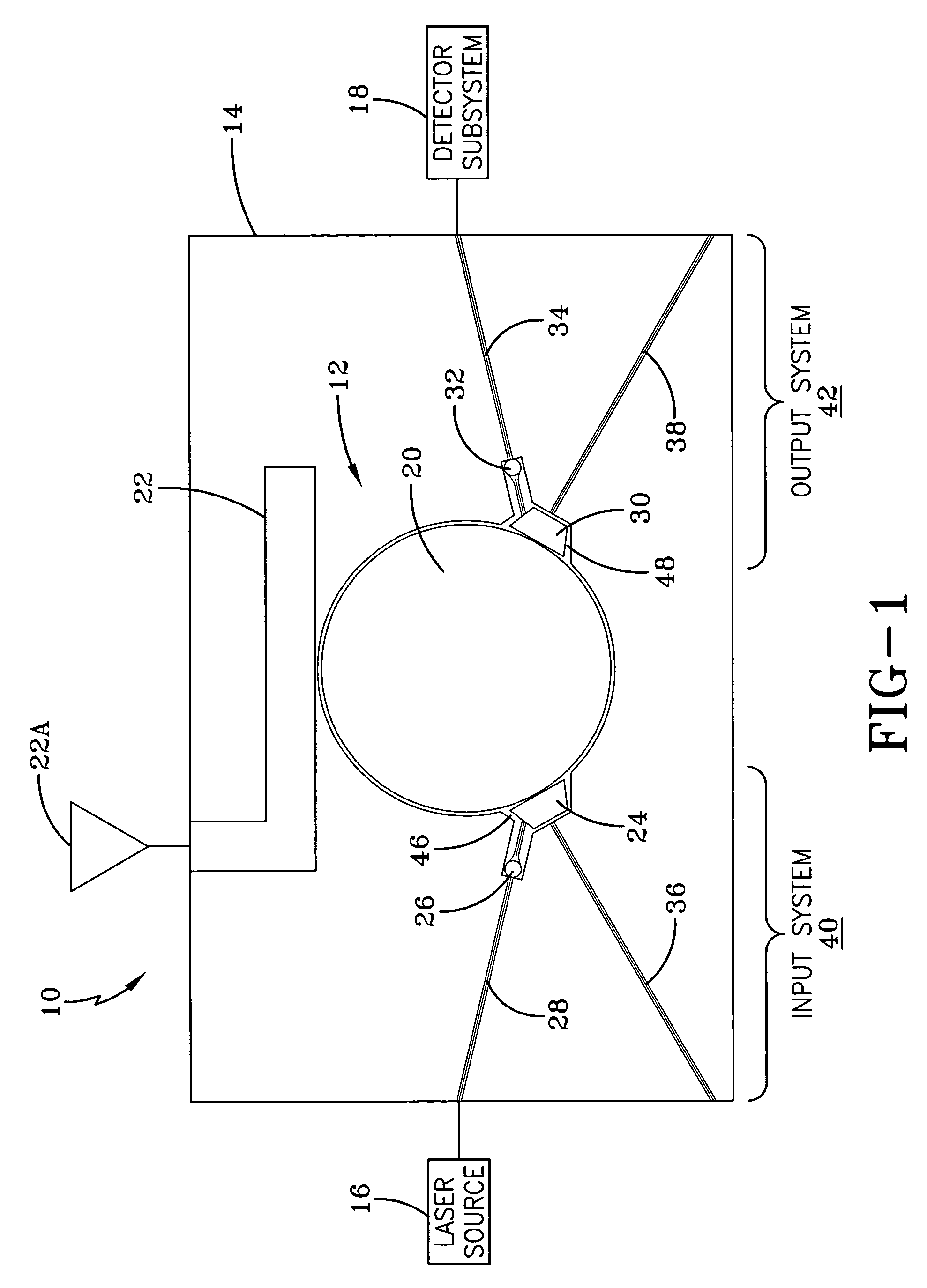
[0024]Referring to the drawings, there is shown in FIG. 1, a schematic of an apparatus 10 used for packing and integrating microphotonic optical devices comprising an optical coupling arrangement 12 and a carrier 14. Microphotonic, photonics, and optical electronics are terms used in the art to describe interactions between optical and electronic physical phenomena. This phenomenon can involve the transforming of electrical signals into optical signals or the reverse. It can also involve the modulation of electronic signals by interaction with the optical signals or the reverse.

[0025]The optical coupling arrangement 12 assists in transferring received RF energy made available, for example, at laser source 16 into light streams comprising optical information, which may be forwarded to a further optical network comprising a detection subsystem 18 shown in FIG. 1.

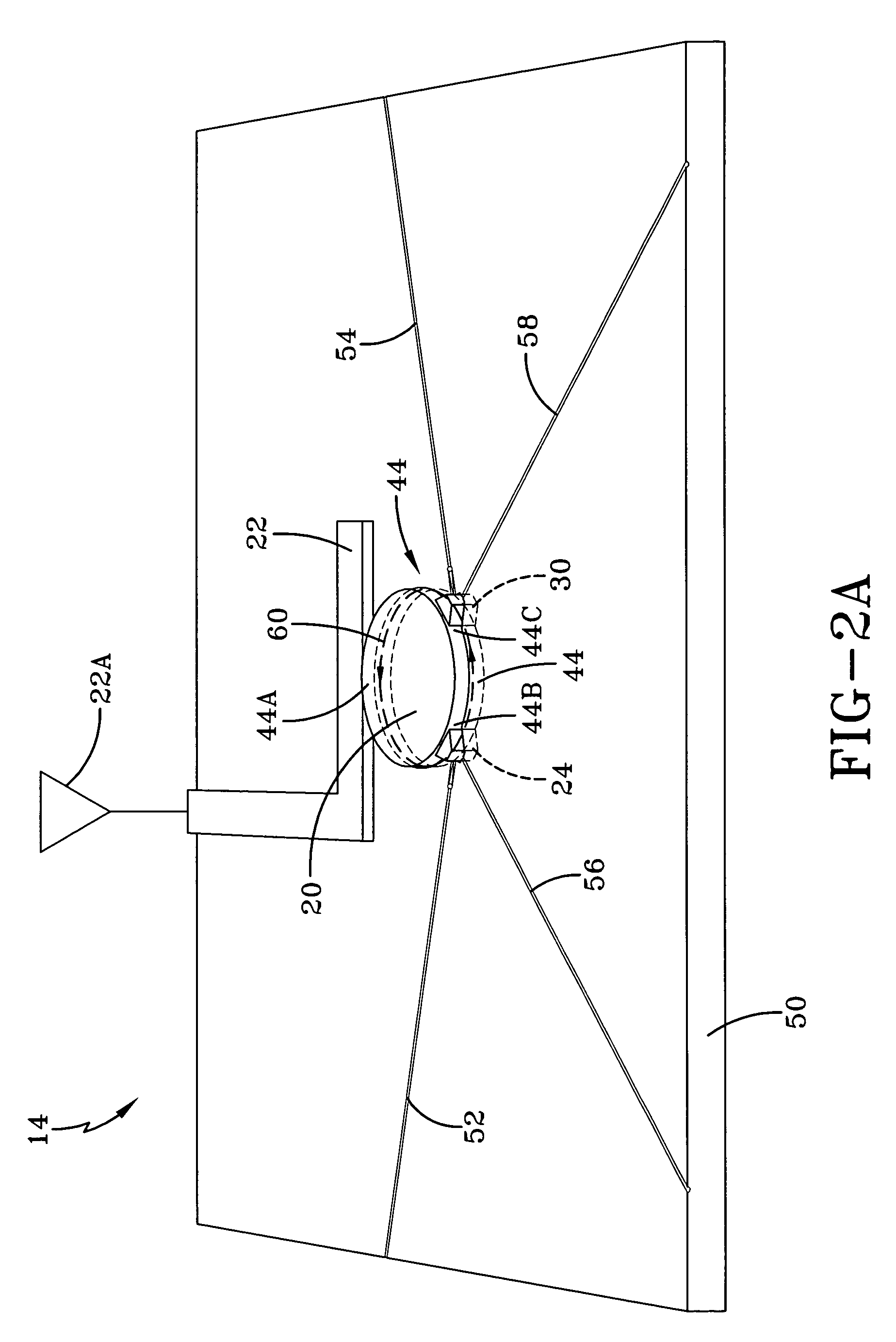
[0026]In the embodiment of FIG. 1, a microphotonic resonator disk 20 preferably comprised of Lithium Niobate has an outwardl...


PUM


Abstract

An apparatus is disclosed that includes a carrier structure and an optical coupling arrangement. The carrier structure is made of a silicon material and allows for the packaging and integrating of microphotonic devices onto a single chip. The optical coupling mechanism enables laser light to be coupled into and out of a microphotonic resonant disk integrated on the carrier. The carrier provides first, second and third cavities that are dimensioned so as to accommodate the insertion and snug fitting of the microphotonic resonant disk and first and second prisms that are implemented by the optical coupling arrangement to accommodate the laser coupling.

Description

ORIGIN OF THE INVENTION[0001]The invention described herein was made by an employee of the United States Government and may be used by or for the Government for governmental purposes without payment of any royalties thereon or therefore.FIELD OF THE INVENTION[0002]The present invention relates to photonics and optoelectronic devices and, more particularly, to packaging microphotonics and optoelectronic devices so that all of these devices will be integrated and interconnected onto a single chip or substrate.BACKGROUND OF THE INVENTION[0003]Microphotonics devices, such as microphotonic resonator disks, and other optoelectronic devices find wide application in microwave technology, such as in converting microwave data transmission having high data rates into optical signals compatible with optical fiber networks. For example, microphotonic resonant disks find application in microphotonic millimeter-wave receivers, based on Lithium Niobate resonator disk technology. Microphotonic reson...

Claims


Application Information

Patent Timeline
Patent Type & Authority Patents(United States)
IPC IPC(8): G02B6/12
CPCG02B6/12004
Inventor NGUYEN, HUNG
Owner UNITED STATES OF AMERICA AS REPRESENTED BY THE ADMINISTATOR OFNAT AERONAUTICS & SPACE ADMINISTATION THE
Why Eureka
Try Eureka