Environmentally protected photonic integrated circuit

a photonic integrated circuit and environment protection technology, applied in the field of environmental protection photonic integrated circuits, can solve the problems of increasing assembly costs, significant part of total costs, and increasing complexity of photonic integrated circuits (pics), for example but not exclusively in the field of optical telecommunication applications, and achieves the effect of adding optical functionality

Active Publication Date: 2022-06-23
EFFECT PHOTONICS BV
View PDF7 Cites 0 Cited by
  • Summary
  • Abstract
  • Description
  • Claims
  • Application Information

AI Technical Summary

Benefits of technology

[0015]In this way, the dielectric protective layer provides both environmental protection of the PIC against environmental contaminants such as for example dust particles and moisture, and additional optical functionality as optical radiation that is carried by the dielectric protective layer of the multilevel optical waveguide assembly can be used for example for at least one of monitoring and testing purposes. In addition, the dielectric protective layer can for example enable mode expansion of the optical radiation in the dielectric protective layer in order to provide low-loss optical coupling between the PIC and an optical fiber. Furthermore, as the dielectric protective layer enables using standard optical fibers instead of specialty or lensed optical fibers that are required in accordance with traditional solutions for establishing optical fiber-chip couplings, the complexity and therefore the costs involved with establishing optical couplings between standard optical fibers and the PIC according to the present invention can be lower than the complexity and costs involved with said traditional solutions.
[0040]According to another aspect of the present invention, an opto-electronic system is provided comprising an environmentally protected photonic integrated circuit according to the invention. The opto-electronic system can for example but not exclusively be used for telecommunication applications. In that case, the opto-electronic systems can be one of a transmitter, a receiver, a transceiver, a coherent transmitter, a coherent receiver and a coherent transceiver. Based on the above, it will be clear that because of the application of the environmentally protected PIC according to the invention, the costs for the opto-electronic system can be reduced.

Problems solved by technology

Photonic integrated circuits (PICs), for example but not exclusively in the field of optical telecommunication applications, are becoming increasingly complex because of the increasing number of optical and electrical functions that are integrated on a single die that preferably has a footprint that is as small as possible.
As a result of the above-mentioned increasing complexity, the costs for assembly and in particular hermetic packaging are a significant part of the total costs of the PICs and the opto-electronic systems in which they are used.

Method used


Image

  • Environmentally protected photonic integrated circuit
  • Environmentally protected photonic integrated circuit
  • Environmentally protected photonic integrated circuit

Examples


Embodiment Construction

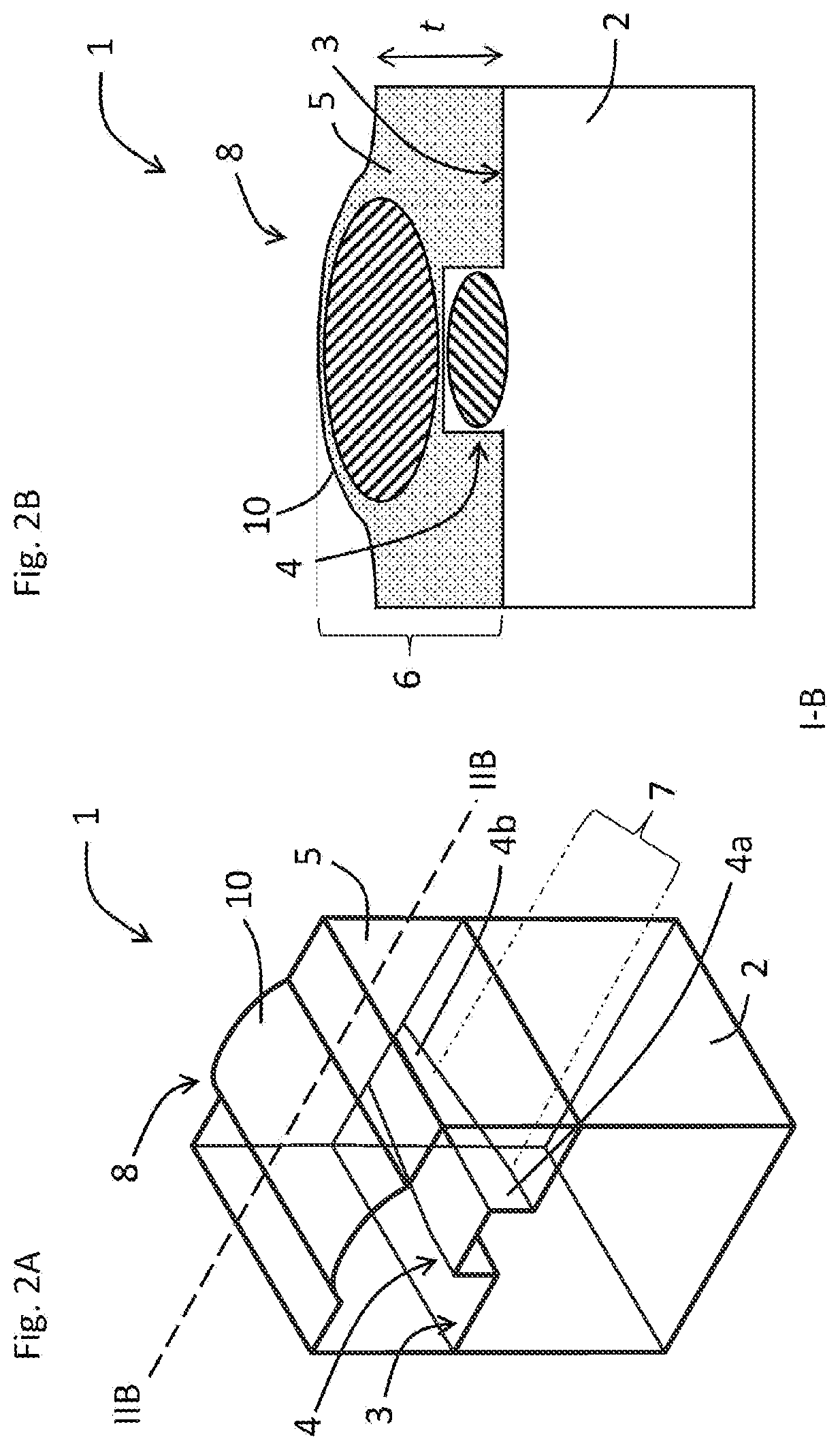
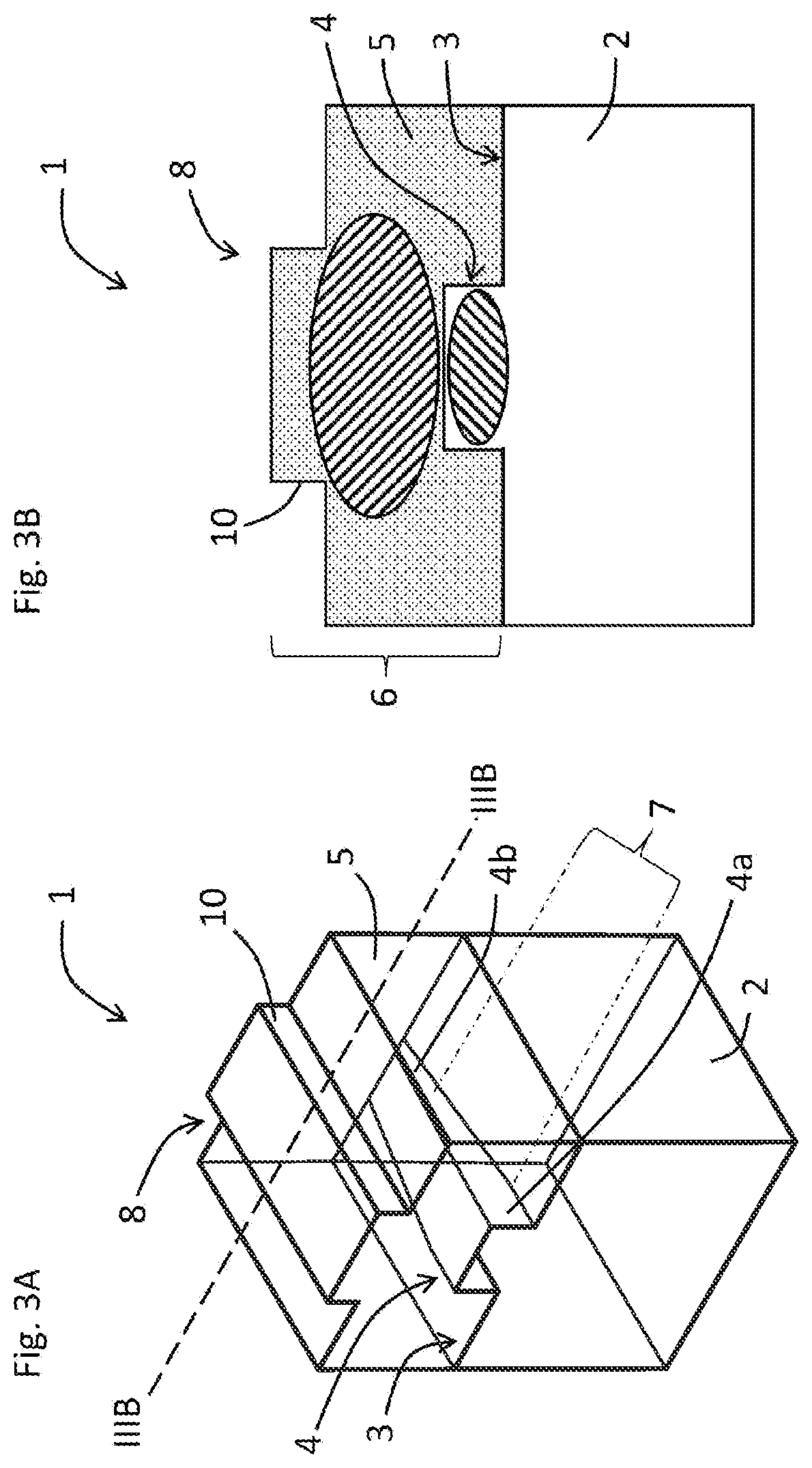
[0061]It is noted that although the presented exemplary, non-limiting embodiments of the environmentally protected PIC 1 according to the present invention involve one polymer-based protective layer, the person skilled in the art will be able to envisage without undue burden embodiments involving more than one polymer-based protective layer and embodiments involving one or more non-polymer-based protective layers, for example silicon-containing layers such as silicon nitride or silicon oxynitride layers, falling within the scope of the present invention.

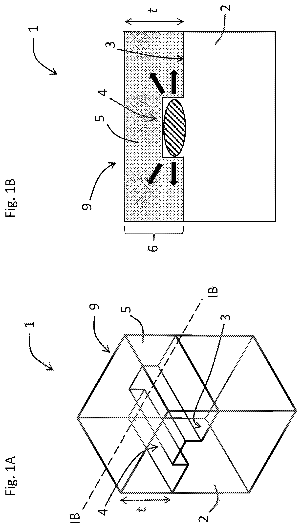
[0062]FIG. 1A shows a schematic isometric view of a part of a first exemplary, non-limiting embodiment of an environmentally protected photonic integrated circuit (PIC) 1 according to the present invention. The PIC 1 comprises an InP-based substrate 2 that has a first surface 3 that is provided with a nonplanar InP-based optical waveguide 4 that is configured to guide optical radiation having a wavelength in a range from for example ...


PUM

PropertyMeasurementUnit
thicknessaaaaaaaaaa
thicknessaaaaaaaaaa
thicknessaaaaaaaaaa

Abstract

An environmentally protected PIC, including an InP-based substrate having a first surface that is at least partially provided with an InP-based optical waveguide, and a dielectric protective layer arranged to cover at least the first surface of the InP-based substrate and the InP-based optical waveguide. The dielectric protective layer is configured to protect said PIC from environmental contaminants, to enable confinement of optical radiation in the dielectric protective layer in at least one direction that is transverse to a direction of propagation of the optical radiation, and to allow exchange of the optical radiation between the InP-based optical waveguide and the dielectric protective layer. An opto-electronic system including PIC.

Description

FIELD OF THE INVENTION[0001]The present invention relates to an environmentally protected photonic integrated circuit that can be used for example but not exclusively for telecommunication applications or sensor applications. The invention further relates to an opto-electronic system, which can be used for example but not exclusively for telecommunication applications or sensor applications, wherein the opto-electronic system comprises said photonic integrated circuit.BACKGROUND OF THE INVENTION[0002]Photonic integrated circuits (PICs), for example but not exclusively in the field of optical telecommunication applications, are becoming increasingly complex because of the increasing number of optical and electrical functions that are integrated on a single die that preferably has a footprint that is as small as possible. The most versatile technology platform for PICs for optical telecommunication applications uses wafers comprising indium phosphide-based (InP) semiconductor material...

Claims


Application Information

Patent Timeline
Patent Type & Authority Applications(United States)
IPC IPC(8): G02B6/12
CPCG02B6/12002G02B2006/12076G02B2006/12061G02B6/12G02B6/1221G02B6/2852G02B6/4253G02B2006/12097G02B6/1228
Inventor HOEKSTRA, TSJERK HANS
Owner EFFECT PHOTONICS BV
Why Eureka
Try Eureka