A coupling packaged silicon photonic chip

A silicon photonics and chip technology, applied in the optical field, can solve the problems of high electrical interconnection requirements, high cost, and low coupling efficiency of laser chips

Active Publication Date: 2019-05-31
苏州亿波达光电子科技有限公司
View PDF3 Cites 0 Cited by
  • Summary
  • Abstract
  • Description
  • Claims
  • Application Information

AI Technical Summary

Problems solved by technology

[0006] The present invention provides a coupled and packaged silicon photonic chip that overcomes the above-mentioned problems or at least partially solves the above-mentioned problems. High interconnection requirements, high cost, and low coupling efficiency

Method used


Image

  • A coupling packaged silicon photonic chip
  • A coupling packaged silicon photonic chip
  • A coupling packaged silicon photonic chip

Examples


Embodiment 1

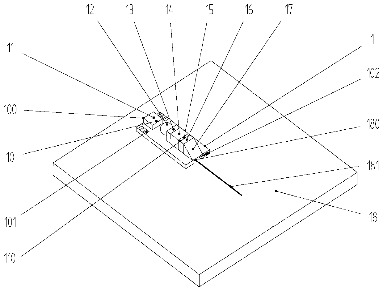
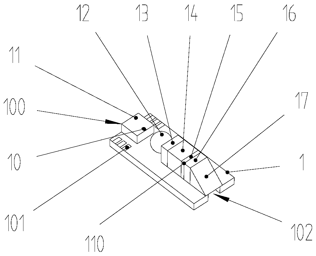
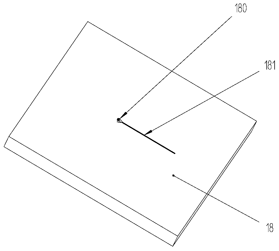
[0026] A coupling and packaging silicon photonic chip, including a substrate 1, a laser chip sub-board 100, a micro-optical module 110, and a silicon photonic chip 18; the laser chip sub-board 100 and the micro-optical module 110 are respectively connected to the substrate 1 , the end of the substrate 1 close to the micro-optical module 110 is provided with a groove 102 for transmitting laser light; the laser chip sub-board 100 is used to emit laser light waves, and the micro-optical module 110 is used The light wave is converted into a TE wave and transmitted to the groove 102; the substrate 1 is connected to the silicon photonic chip 18, and the optical coupling grating 180 of the silicon photonic chip 18 is arranged in the groove 102 in the TE wave transmission direction place.

[0027] In this embodiment, the laser chip sub-board 100 includes a laser chip 10 and a heat sink 11 , and the laser chip 10 is bonded to the heat sink 11 through AuSn eutectic bonding.

[0028] In...

Embodiment 2

[0038] A coupling and packaging silicon photonic chip, including a substrate 1, a laser chip sub-board 100, a micro-optical module 110, and a silicon photonic chip 18; the laser chip sub-board 100 and the micro-optical module 110 are respectively connected to the substrate 1 , the end of the substrate 1 close to the micro-optical module 110 is provided with a groove 102 for transmitting laser light; the laser chip sub-board 100 is used to emit laser light waves, and the micro-optical module 110 is used The light wave is converted into a TE wave and transmitted to the groove 102; the substrate 1 is connected to the silicon photonic chip 18, and the optical coupling grating 180 of the silicon photonic chip 18 is arranged in the groove 102 in the TE wave transmission direction place.

[0039] In this embodiment, the laser chip sub-board 100 includes a laser chip 10 and a heat sink 11 , and the laser chip 10 is bonded to the heat sink 11 through AuSn eutectic bonding.

[0040] In...


PUM


Abstract

The invention provides a coupled-packaged silicon photon chip comprising a substrate, a laser chip daughter board, a micro-optical module group, and a silicon photon chip. The laser chip daughter board and the micro-optical module group are respectively connected to the substrate. A groove for transmitting laser light is formed in one end, being close to the micro-optical module group, of the substrate. The laser chip daughter board is used for emitting a laser light wave; and the micro-optical module group is configured to convert the laser light wave into a TE wave and transmit the TE wave to the groove. The substrate is connected to the silicon photon chip; and an optical path coupling grating of the silicon photon chip is arranged at a TE wave transmission direction in the groove. Therefore, the back propagation of the interface light wave can be reduced to protect the laser chip; the low-loss coupling of the laser chip and the silicon photon chip is realized; the structure is compact and the size is small; the silicon-photon-wafer-level bonding packaging is realized; and the laser is outputted in a TE wave manner; and no mode converter needs to be manufactured on the silicon photonic wafer.

Description

technical field [0001] The invention relates to the field of optical technology, and more specifically, to a coupled and packaged silicon photonic chip. Background technique [0002] Silicon photonics technology refers to the fabrication of optical devices, photonic integrated circuits and optoelectronic integrated circuits on silicon-based materials to achieve signal transmission and processing. Silicon photonic devices have a wide range of uses and a large application span, from metropolitan area networks such as communications with a length of more than 1,000 kilometers, from optical access networks to LAN / storage networks, from device-level backplane interconnection to board-level chips Interconnects, even on-chip interconnects, have a wide range of applications. At present, silicon photonic chips can process data at a speed of 300Gbps per square millimeter, which is 10 times or even 50 times faster than existing standard processors. [0003] The basic elements of opti...

Claims


Application Information

Patent Timeline
Patent Type & Authority Patents(China)
IPC IPC(8): G02B6/42
CPCG02B6/4204G02B6/4251G02B6/4269G02B6/4296
Inventor 郑煜郜飘飘夏冰心吴雄辉开小超严一雄段吉安
Owner 苏州亿波达光电子科技有限公司
Why Eureka
Try Eureka