Asymmetric waveguide optical fiber end face coupler with two unequal-height arms based on mode evolution

An asymmetric waveguide and fiber end face technology, which is applied in the coupling of optical waveguides, optical waveguides and optical guides, instruments, etc., can solve the problem that the coupling structure cannot be well realized in the height direction, and it is difficult to achieve polarization insensitivity and coupling efficiency. problems such as rise, to achieve the effect of large tolerance, compact structure, and enlarged mold spot size

Active Publication Date: 2021-09-07
ZHEJIANG UNIV
View PDF9 Cites 0 Cited by
  • Summary
  • Abstract
  • Description
  • Claims
  • Application Information

AI Technical Summary

Problems solved by technology

The scheme of grating coupling: Although this scheme can achieve relatively simple coupling, facilitate wafer testing and packaging, and has low requirements on the process, due to the limitation of its physical mechanism, it is difficult to achieve polarization insensitivity and wide bandwidth. Small, the coupling efficiency is difficult to rise to a new height
However, for the currently commonly used end face coupling scheme, limited by the technological level, it can only realize the coupling with gradual changes in the width direction, that is, the traditional ta

Method used


Image

  • Asymmetric waveguide optical fiber end face coupler with two unequal-height arms based on mode evolution
  • Asymmetric waveguide optical fiber end face coupler with two unequal-height arms based on mode evolution
  • Asymmetric waveguide optical fiber end face coupler with two unequal-height arms based on mode evolution

Examples


specific Embodiment

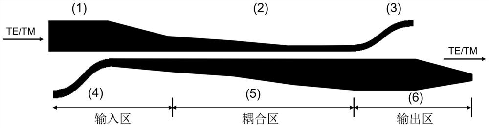
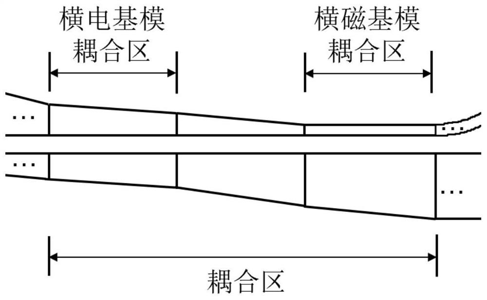
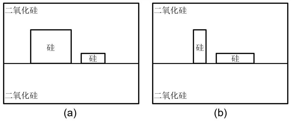
[0060] The silicon nanowire optical waveguide based on silicon-on-insulator (SOI) material is selected: the core layer is silicon material, the thickness of the high-arm waveguide is 220nm, and the refractive index is 3.5068; the thickness of the short-arm waveguide is 150nm, the refractive index is 3.5068, and the lower cladding , the upper cladding material is SiO 2 , with a thickness of 2 μm and a refractive index of 1.444. Considering that the central wavelength is 1310nm and the number of modes is 2, including the fundamental transverse electric mode and the transverse magnetic fundamental mode, the device structure diagram is as follows figure 1 shown.

[0061] For the high-arm input wide straight waveguide 1, the width is 0.38 μm and the length is 10 μm; the beginning and end widths of the short-arm input S-shaped narrow curved waveguide 4 are both 0.18 μm to meet most current technological requirements. The short-arm input S-shaped narrow curved waveguide 4 has a len...


PUM


Abstract

The invention discloses an asymmetric waveguide optical fiber end face coupler with two unequal-height arms based on mode evolution. A high-arm waveguide is composed of an input wide straight waveguide, a conical coupling waveguide group and an output narrow bent waveguide which are connected in sequence, and a low-arm waveguide is composed of an input narrow bent waveguide, a conical coupling waveguide group and an output conical waveguide which are connected in sequence; the width of the high-arm waveguide is gradually reduced, and the width of the low-arm waveguide is gradually increased; a certain distance exists between the two arm waveguides, and then the distance between the high-arm waveguide and the low-arm waveguide gradually approaches until the distance is kept unchanged and then the distance is increased; and a transverse electric fundamental mode and a transverse magnetic fundamental mode are input through the high-arm input waveguide, evolve in the two-arm waveguide to form a super mode, are finally coupled into the low-arm waveguide, are output through the conical waveguide and are subjected to end face coupling with an optical fiber. The asymmetric waveguide optical fiber end face coupler can effectively enlarge the size of the spot size, and has the advantages of large bandwidth, large tolerance, compact structure and the like.

Description

technical field [0001] The invention relates to an on-chip waveguide fiber end-face coupler, in particular to a mode evolution-based asymmetrical waveguide fiber end-face coupler with two arms of unequal height that realizes high coupling efficiency and large bandwidth. Background technique [0002] A waveguide fiber coupler refers to coupling a mode from an optical fiber to an on-chip optical waveguide. It is essentially a mode spot converter that converts a larger mode spot in the fiber into a smaller mode spot in the waveguide. With the continuous development of on-chip optical communication technology, there is an increasing demand for effectively coupling an on-chip optical signal into an optical fiber. [0003] In terms of the performance requirements of the waveguide fiber coupler, on the one hand, it has high requirements for high coupling efficiency, which can meet the needs of various communication systems; on the other hand, the on-chip waveguide fiber coupler is ...

Claims


Application Information

Patent Timeline
IPC IPC(8): G02B6/30G02B6/122G02B6/12
CPCG02B6/305G02B6/1228G02B6/12004G02B2006/12147
Inventor 戴道锌易晓琳
Owner ZHEJIANG UNIV
Why Eureka
Try Eureka