Two-dimensional side coupling photonic crystal waveguide single-channel system

A photonic crystal waveguide and side-coupling technology, applied in the directions of light guides, optics, optical components, etc., can solve the problems of difficulty in controlling the distance parameters between the graded optical fiber and the photonic crystal device, the influence of integration, and limitations, and achieve compact structure and low bending loss. , the effect of high integration

Inactive Publication Date: 2013-01-23
CHANGCHUN INST OF OPTICS FINE MECHANICS & PHYSICS CHINESE ACAD OF SCI
View PDF9 Cites 0 Cited by
  • Summary
  • Abstract
  • Description
  • Claims
  • Application Information

AI Technical Summary

Problems solved by technology

The evanescent wave method also faces some problems, such as the processing of a specific graded fiber, the difficulty in controlling the distance parameters between the graded fiber used in the coupling process and the photonic crystal device, and the need for a sophisticated external calibration and adjustment system and an external calibration adjustment system The impact on the integration degree and other issues limit the application of the evanescent wave coupling method

Method used


Image

  • Two-dimensional side coupling photonic crystal waveguide single-channel system
  • Two-dimensional side coupling photonic crystal waveguide single-channel system
  • Two-dimensional side coupling photonic crystal waveguide single-channel system

Examples


specific Embodiment approach 1

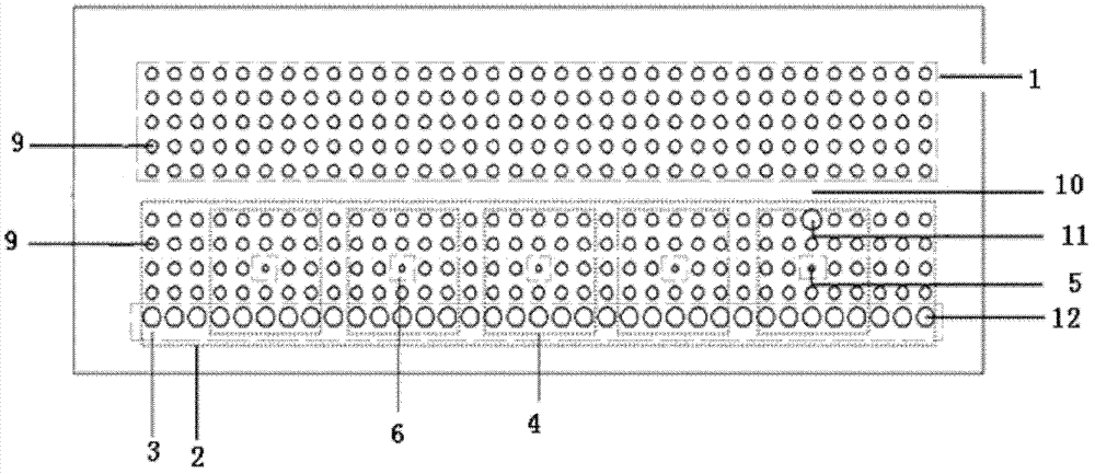
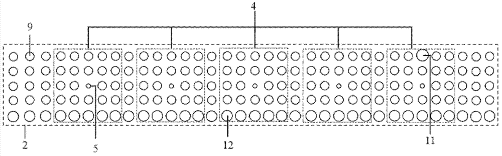
[0018] Specific implementation mode one, combination Figure 1 to Figure 5 To illustrate this embodiment, the two-dimensional side-coupled photonic crystal waveguide single-channel system of this embodiment includes a waveguide layer 13, a low refractive index buried layer 7, and a substrate layer 8. The waveguide layer is located on the low refractive index buried layer 7. On the upper part, the lower part of the low refractive index buried layer 7 is connected to the substrate layer 8; the waveguide layer includes a waveguide first region 1, a defect region 10, and a waveguide second region 2; a defect region is distributed at the junction of the waveguide first region 1 and the waveguide second region 2 10. The first area 1 of the waveguide is composed of a plurality of dielectric pillars 9 periodically arranged, the outermost row of the second area 2 of the waveguide is distributed with coupling dielectric pillars 12, and this row of coupling dielectric pillars 12 constitutes...

specific Embodiment approach 2

[0034] Specific implementation mode two, combination Figure 6 to Figure 9 To describe this embodiment, the specific manufacturing process of the two-dimensional side-coupled photonic crystal waveguide single-channel system described in this embodiment and specific implementation 1:

[0035] The first step is to prepare the dicing groove required for dicing: such as Image 6 As shown in a~6g.

[0036] (A) The counter substrate silicon 101 is 600 μm thick, on which a 3 μm thick silicon dioxide layer 102 is grown (such as Image 6 a) Carry out cleaning treatment;

[0037] (B) such as Image 6 As shown in b, a strontium titanate film 103 is prepared on the silicon dioxide layer 102 by a sol-gel method;

[0038] (C) such as Image 6 As shown in c, a photoresist film 104 with a thickness of 2-3 μm is coated on the strontium titanate film 103;

[0039] (D) Put the completed structure in step (C) into an oven before baking;

[0040] (E) such as Image 6 As shown in d, ultraviolet exposure is p...


PUM


Abstract

A two-dimensional side coupling photonic crystal waveguide single-channel system relates to a microstructure photonic crystal element in the technical field of optics, which can achieve efficient coupling between photonic crystal waveguide and a traditional optical device or an externally-arranged light source. The two-dimensional side coupling photonic crystal waveguide single-channel system adopts a mode that a plurality of photonic crystal resonant cavities are connected in parallel. An electromagnetic wave enters a coupling system formed by parallelly connecting the plurality of photonic crystal resonant cavities from a coupling area in a waveguide second area. The electromagnetic wave with the same waveguide response frequency with the parallelly connected photonic crystal resonant cavities and photonic crystal and photonic crystals enters a defect area through efficient coupling of the plurality of parallelly connected photonic crystal resonant cavities, achieves one-sided transmission in the defect area and emits out through one side of the photonic crystal waveguide, thereby achieving the purpose of improving coupling area. The coupling efficiency is high, and the photoniccrystal waveguide is compact in structure, small in size and high in integration level.

Description

Technical field [0001] The invention relates to a microstructure photonic crystal element in the field of optical technology, in particular to a two-dimensional side-coupled photonic crystal waveguide single channel system and a manufacturing method thereof. Background technique [0002] Photonic crystals are artificial microstructures formed by substances with different dielectric constants arranged periodically in space. In recent years, optoelectronic functional devices based on photonic crystal materials have received extensive attention. Taking advantage of the photonic band gap and photonic local characteristics of photonic crystals, photonic crystal waveguides, filters, optical switches, couplers and other photonic crystal optoelectronic devices have been seen. The report laid a good foundation for the realization of large-scale optoelectronic integration and all-optical networks in the future. [0003] Photonic crystals are artificial microstructures periodically arranged ...

Claims


Application Information

Patent Timeline
Patent Type & Authority Patents(China)
IPC IPC(8): G02B6/122
Inventor 王维彪梁中翥梁静秋崔乃迪
Owner CHANGCHUN INST OF OPTICS FINE MECHANICS & PHYSICS CHINESE ACAD OF SCI
Why Eureka
Try Eureka