Method and system for providing a thin film with a controlled crystal orientation using pulsed laser induced melting and nucleation-initiated crystallization

a technology of controlled crystal orientation and laser induced melting, applied in the direction of crystal growth process, polycrystalline material growth, manufacturing tools, etc., can solve the problems of reducing the electro-migration rate, increasing the electro-migration rate, and reducing the production efficiency of metal thin films

Inactive Publication Date: 2008-07-15
THE TRUSTEES OF COLUMBIA UNIV IN THE CITY OF NEW YORK
View PDF129 Cites 29 Cited by
  • Summary
  • Abstract
  • Description
  • Claims
  • Application Information

AI Technical Summary

Problems solved by technology

An inherent problem in the production of metallic thin films is minimizing the electro-migration that occurs in the metal interconnects.
These grains may extend in a direction which is parallel to the direction of the interconnect lines, i.e., along the direction of the current flow, which is considered to be particularly undesirable (i.e., such grain direction results in an increased electro-migration).
Therefore, the void may become so large that an open circuit or a break in the interconnect line results.
If the protrusion becomes large enough, a contact with an adjacent interconnect may occur, thereby causing an undesired connection between the adjacent interconnect lines.

Method used


Image

  • Method and system for providing a thin film with a controlled crystal orientation using pulsed laser induced melting and nucleation-initiated crystallization
  • Method and system for providing a thin film with a controlled crystal orientation using pulsed laser induced melting and nucleation-initiated crystallization
  • Method and system for providing a thin film with a controlled crystal orientation using pulsed laser induced melting and nucleation-initiated crystallization

Examples


Embodiment Construction

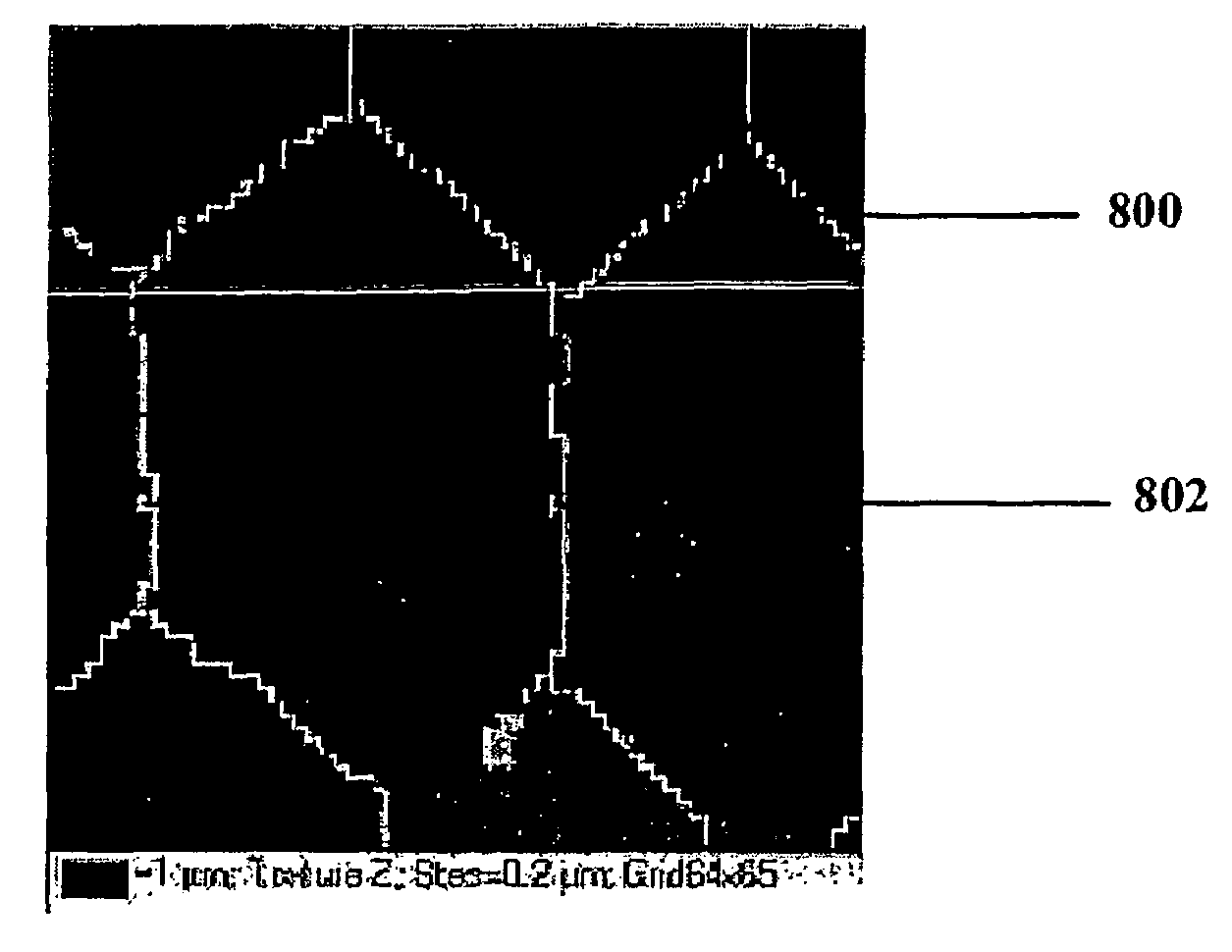
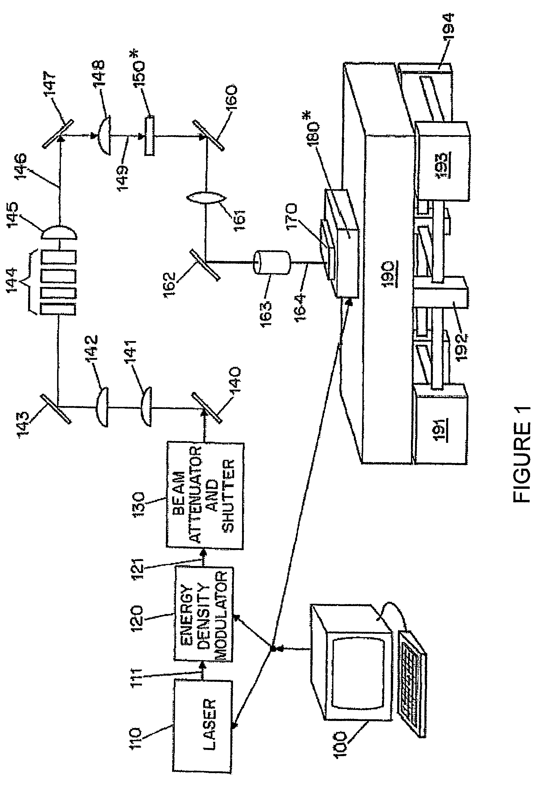
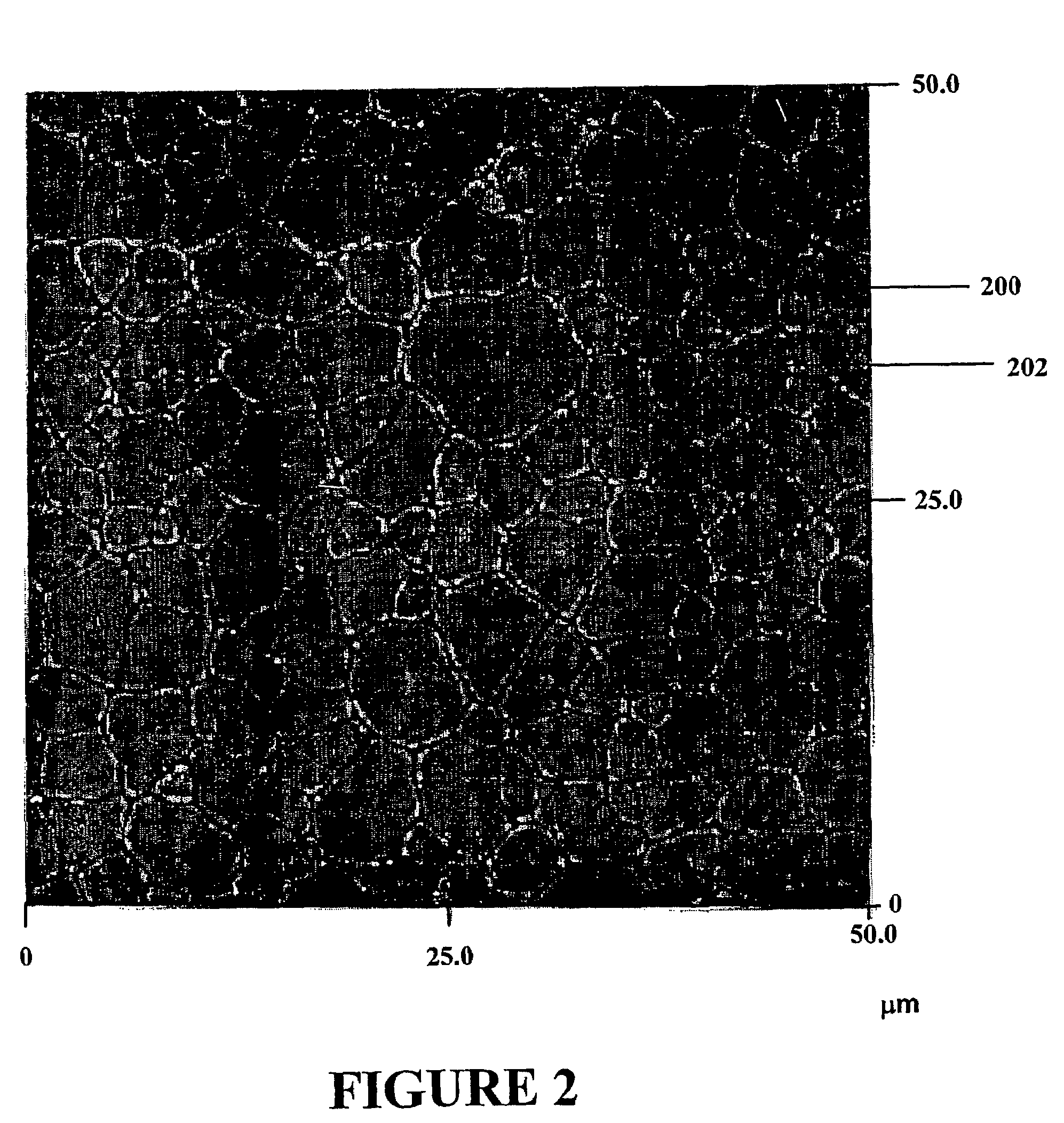
[0023]In one exemplary embodiment of the present invention, a uniform crystalline orientation of at least one section of a metal thin film may be obtained using the sequential lateral solidification process. Therefore, in order to fully understand the present invention, the sequential lateral solidification process is further described. As disclosed in aforementioned patent applications, the sequential lateral solidification (“SLS ”) process is a technique for producing large grained thin films through small-scale unidirectional translation of a sample between sequential pulses emitted by an excimer laser. As each pulse is absorbed by the sample, a small area of the sample is caused to melt completely, and then resolidify laterally into a crystal region produced by the preceding pulses of a pulse set. It should be understood that various systems according to the present invention may be utilized to generate, nucleate, solidify and crystallize one or more areas on the thin film (e.g....


PUM

PropertyMeasurementUnit
thicknessaaaaaaaaaa
shapeaaaaaaaaaa
temperatureaaaaaaaaaa

Abstract

Method and system for generating a metal thin film with a uniform crystalline orientation and a controlled crystalline microstructure are provided. For example, a metal layer is irradicated with a pulsed laser to completely melt the film throughout its entire thickness. The metal layer can then resolidify to form grains with a substantially uniform orientation. The resolidified metal layer can be irradiated with a sequential lateral solidification technique to modify the crystalline microstructure (e.g., create larger grains, single-crystal regions, grain boundary controlled microstructures, etc.) The metal layer can be irradiated by patterning a beam using a mask which includes a first region capable of attenuating the pulsed laser and a second region allowing complete irradiation of sections of the thin film being impinged by the masked laser beam. An inverse dot-patterned mask can be used, the microstructure that may have substantially the same as the geometric pattern as that of the dots of the mask.

Description

CROSS REFERENCE TO RELATED APPLICATION(S)[0001]The present application is a continuation of International Patent Application No. PCT / US03 / 09861, filed Apr. 1, 2003, published on Oct. 16, 2003 as International Patent Publication No. WO 03 / 084688, which claims priority to U.S. Provisional Application Ser. No. 60 / 369,186, filed on Apr. 1, 2002, the contents of which hereby incorporated by reference in their entireties herein.NOTICE OF GOVERNMENT RIGHTS[0002]The U.S. Government may have certain rights in this invention pursuant to the terms of the Defense Advanced Research Project Agency award number N66001-9S-1-8913.FIELD OF THE INVENTION[0003]The present invention relates to a system and process for producing a metal thin film having a uniform crystal orientation and controlled microstructure. In particular, the system and process of the present invention utilize a pulsed laser beam in conjunction with sequential lateral solidification (“SLS”) techniques to produce, e.g., an aluminum ...

Claims


Application Information

Patent Timeline
Patent Type & Authority Patents(United States)
IPC IPC(8): H01L21/00H01L21/31B21CB23K26/00C07C19/08C09K19/34H01L21/84H05H1/24
CPCB23K26/0656C30B13/24H01L21/76867H01L21/76838C30B29/02B23K26/066
Inventor IM, JAMES S.CHOI, JAE BEOM
Owner THE TRUSTEES OF COLUMBIA UNIV IN THE CITY OF NEW YORK
Why Eureka
Try Eureka