Image display device, and display panel and driving method thereof, and pixel circuit

a display device and display panel technology, applied in static indicating devices, solid-state devices, instruments, etc., can solve the problems of increasing power consumption and securing the charging time of data lines, and achieve the effect of preventing unnecessary current flowing

Inactive Publication Date: 2008-07-22
SAMSUNG DISPLAY CO LTD
View PDF36 Cites 26 Cited by
  • Summary
  • Abstract
  • Description
  • Claims
  • Application Information

AI Technical Summary

Benefits of technology

[0012]In one exemplary embodiment of the present invention, there is provided an image display device that compensates for the threshold voltage of the driving transistor and prevents an unnecessary current flowing to the display element. In said one exemplary embodiment, a transistor may be added between the driving transistor and the display element.

Problems solved by technology

The voltage programming method is for displaying an image by applying a data voltage representing gradation to the pixel circuit, but may have a problem of non-uniformity due to a deviation of the threshold voltage of the driving transistor and the electron mobility.
But, this method is problematic in securing the time for charging the load of the data lines, since only a slight quantity of current is used in controlling the organic EL element.
Moreover, the current flows to the OLED while the data voltage is transferred to the gate of the driving transistor M1 and charged in the capacitor Cst, thereby increasing power consumption.

Method used


Image

  • Image display device, and display panel and driving method thereof, and pixel circuit
  • Image display device, and display panel and driving method thereof, and pixel circuit
  • Image display device, and display panel and driving method thereof, and pixel circuit

Examples


Embodiment Construction

[0030]In the following detailed description, exemplary embodiments of the present invention are shown and described, by way of illustration. As those skilled in the art would recognize, the described embodiments may be modified in various different ways, all without departing from the spirit or scope of the present invention. Accordingly, the drawings and description are to be regarded as illustrative in nature, and not restrictive.

[0031]The parts not related to the description are omitted in the Figures for more definite description of the present invention. When a component is described as being coupled to another component it refers to cases where the two components are directly coupled to each other, and additionally to cases where the two components are coupled to each other with a third element between them.

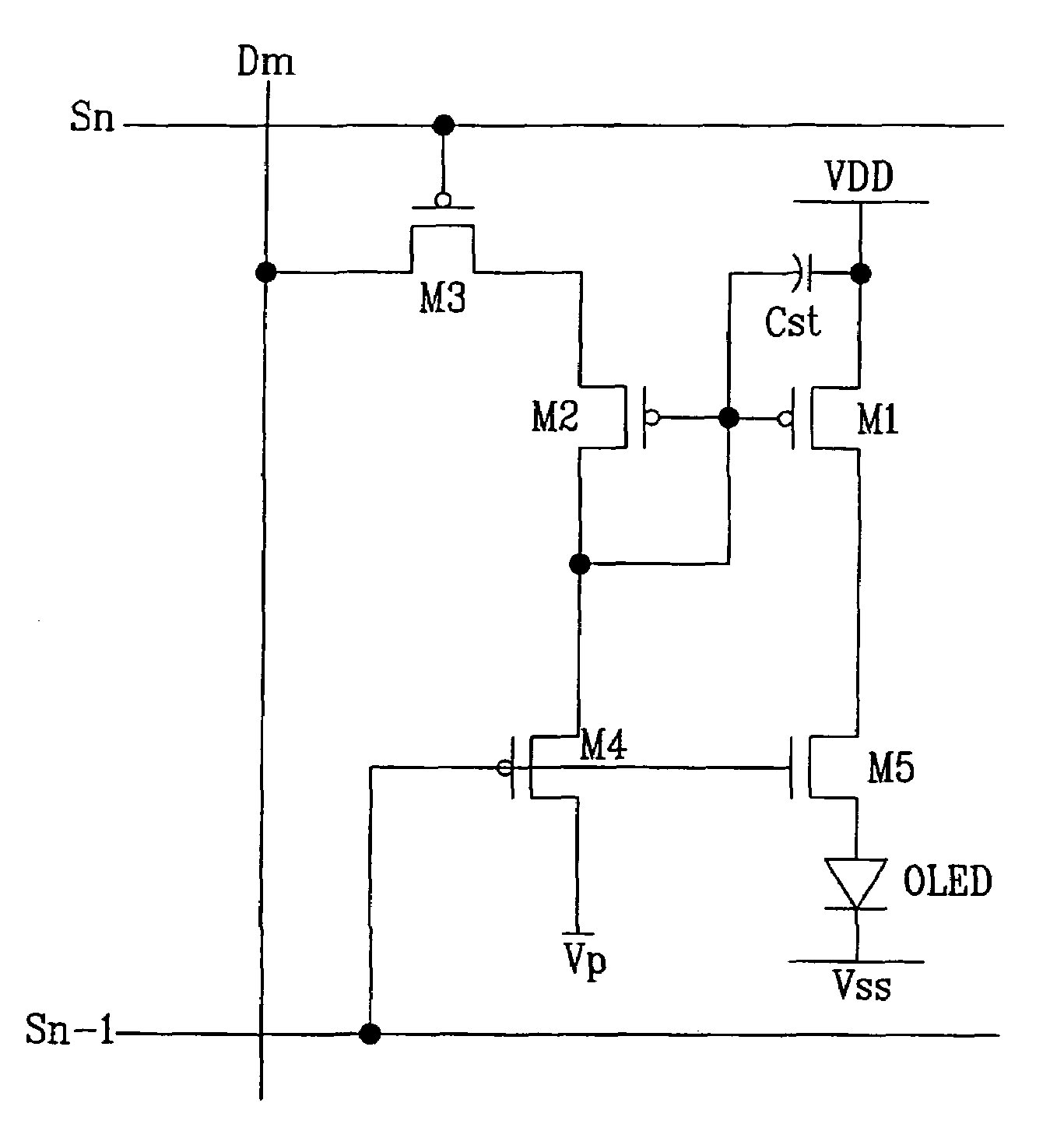
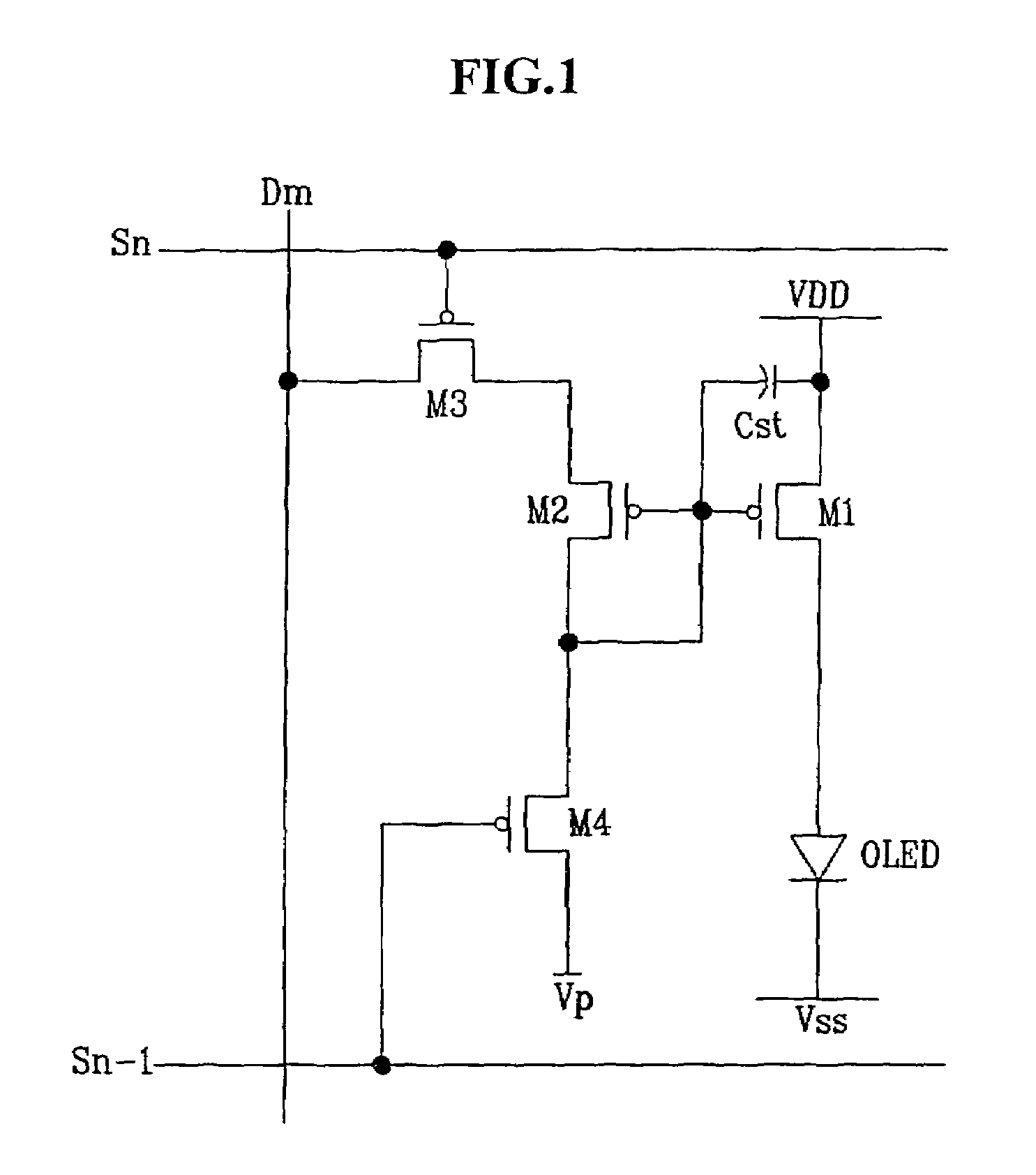
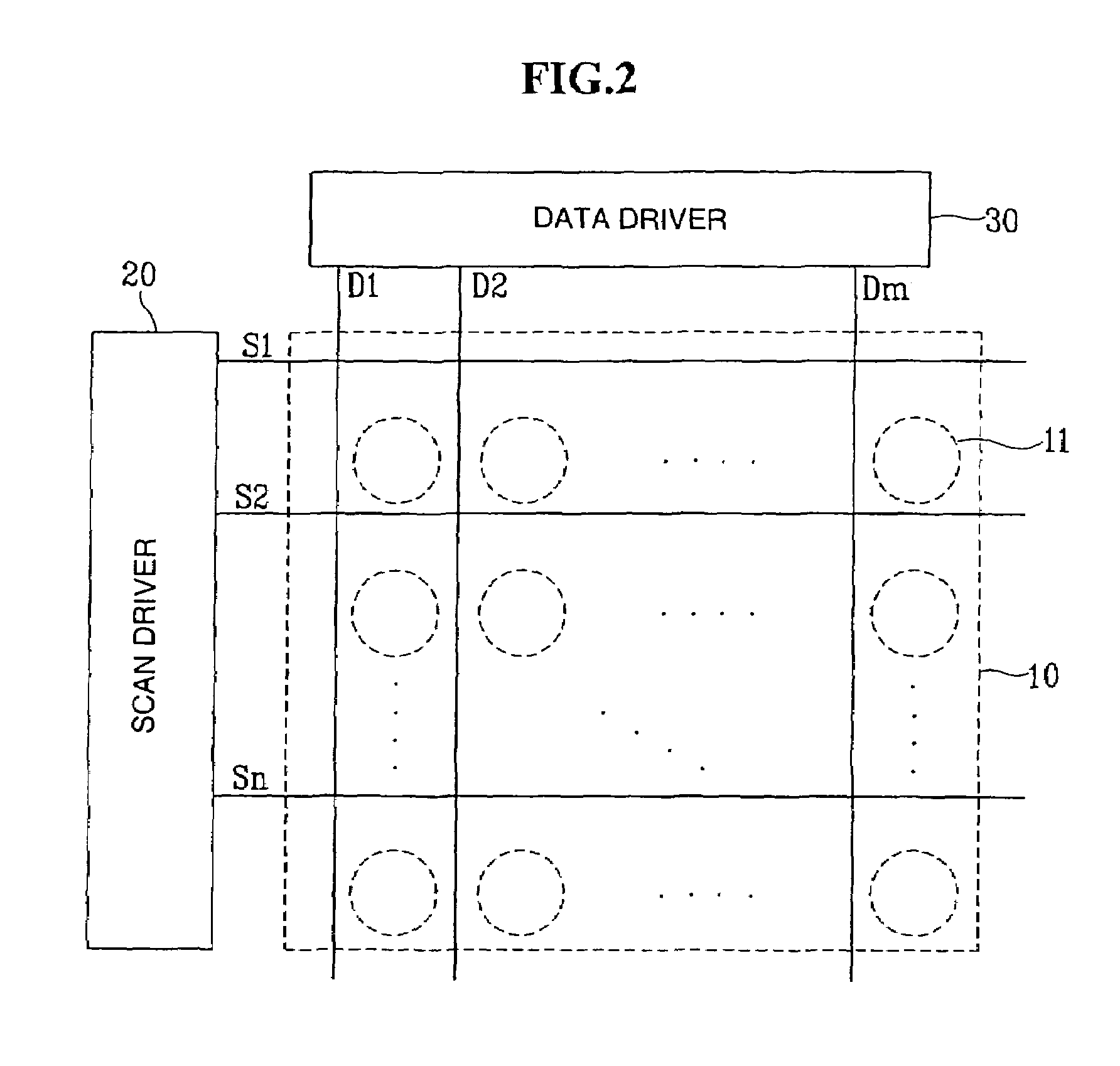
[0032]Now, reference will be made to FIG. 2 in the description of an organic EL display device according to an exemplary embodiment of the present invention. FIG. 2 is a sc...


PUM


Abstract

In a pixel circuit of an organic EL display device, a gate of a driving transistor is coupled to a gate of a compensating transistor, which is configured to operate as a diode. A precharge voltage is applied to the gate of the driving transistor while a selection signal is applied to a previous scan line, so that the compensating transistor is biased in a forward direction to apply a data voltage on the gate of the drive transistor. The driving transistor may be electrically isolated from the organic EL element (OLED) while precharging, so as to prevent the OLED from emitting a light using the precharge voltage. In addition, the driving transistor may be electrically isolated from the OLED while the data voltage is being charged, so as to prevent the OLED from emitting a light.

Description

CROSS REFERENCE TO RELATED APPLICATION[0001]This application claims priority to and the benefit of Korean Patent Application No. 2003-0027604 filed on Apr.30, 2003 in the Korean Intellectual Property Office, the content of which is incorporated herein by reference.BACKGROUND OF THE INVENTION[0002](a) Field of the Invention[0003]The present invention relates to an image display device, and a display panel and driving method thereof. More specifically, the present invention relates to an organic electroluminescent (hereinafter, referred to as “EL”) display device.[0004](b) Description of the Related Art[0005]The organic EL display device, which is a display device for electrically exciting a fluorescent organic compound to emit a light, has organic light-emitting cells that are voltage- or current-driven to display an image. These organic light-emitting cells have a structure composed of an anode (indium tin oxide (ITO)) layer, an organic thin film, and a cathode (metal) layer. For a ...

Claims


Application Information

Patent Timeline
Patent Type & Authority Patents(United States)
IPC IPC(8): G09G3/32G09G3/20H01L51/50G09G3/30
CPCG09G3/3233G09G2300/0819G09G2300/0842G09G2300/0861G09G2330/021G09G2310/0262G09G2320/0238G09G2320/043G09G2310/0251G09G3/30
Inventor CHUNG, BO-YONGPARK, YONG-SUNGKWAK, WON-KYUOH, CHOON-YULYANG, SUN-ARYU, DO-HYUNG
Owner SAMSUNG DISPLAY CO LTD
Why Eureka
Try Eureka