Carrier-based electronic module

a carrier-based, electronic module technology, applied in the direction of printed circuit manufacturing, printed circuit non-printed electric components association, printed circuit aspects, etc., can solve the problems of increasing the main memory of the computer, requiring complex three-dimensional stacking of chips, and not meeting the demand, so as to increase the memory density of the memory module and efficiently utilize the available real estate

Inactive Publication Date: 2008-07-29
LEGACY ELECTRONICS INC
View PDF117 Cites 62 Cited by
  • Summary
  • Abstract
  • Description
  • Claims
  • Application Information

AI Technical Summary

Benefits of technology

[0020]The invention may be utilized to increase memory density on memory modules. For other types of IC packages, it may be employed to more efficiently utilize available real estate on a printed circuit board.

Problems solved by technology

When such memory is relatively inexpensive compared to the overall cost of a computer system, an almost unsatiable demand results, with computer manufacturers tending to install an amount of main memory in each system that greatly exceeds the amount required for average program use.
On the other hand, when it is costly, manufacturers typically install an amount in each system that only marginally fulfills the requirement of the average program.
Although the sales prices of computers may, thus, be maintained at low levels, the end user may soon find that he must upgrade his computer's main memory.
As a general rule, the three-dimensional stacking of chips requires complex, non-standard packaging methods.
As can be seen by the foregoing examples, increased chip density is achieved through the use of complicated packaging and stacking arrangements, which must necessarily be reflected in a higher costs per bit of storage.

Method used


Image

  • Carrier-based electronic module
  • Carrier-based electronic module
  • Carrier-based electronic module

Examples


first embodiment

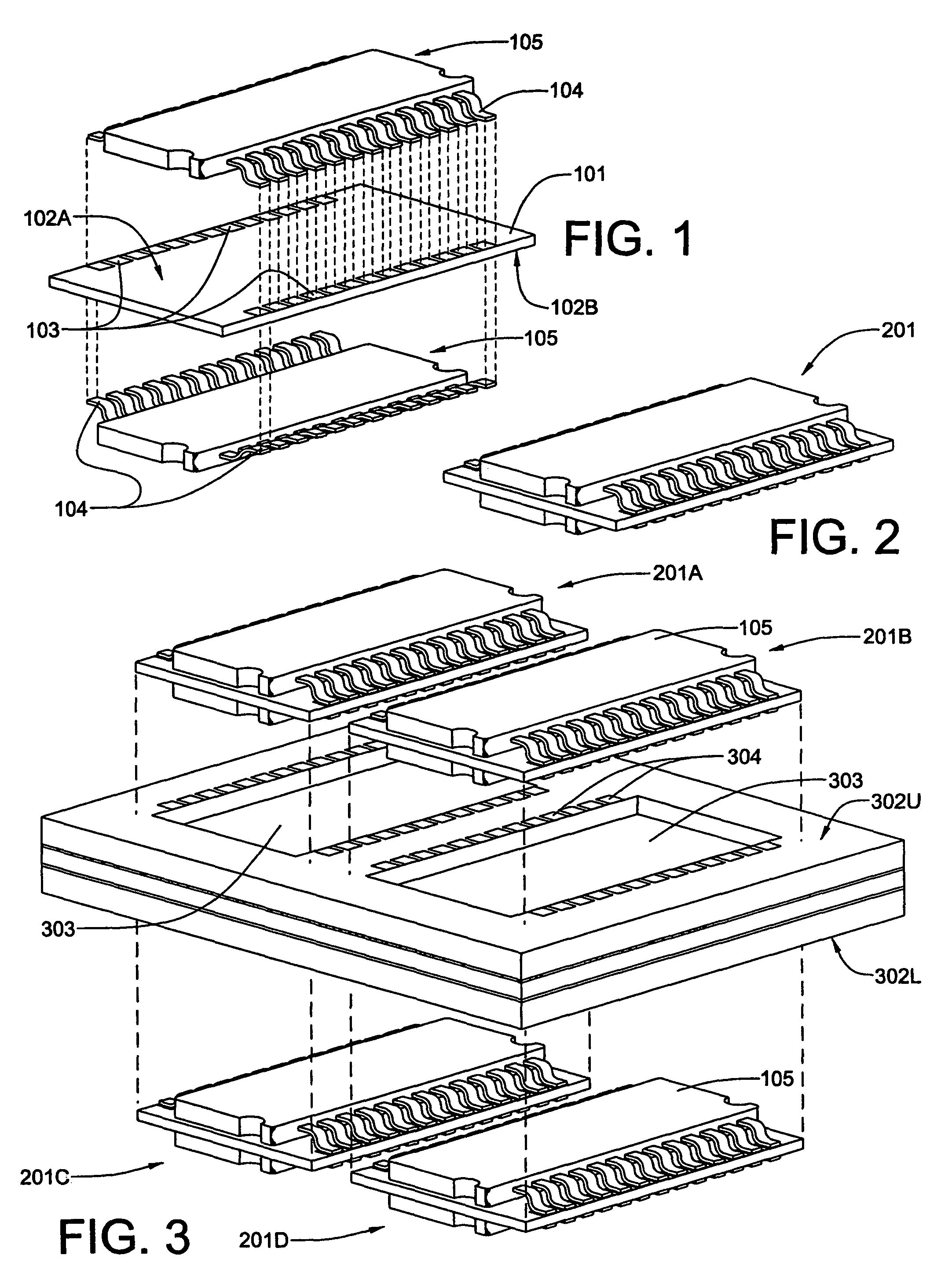
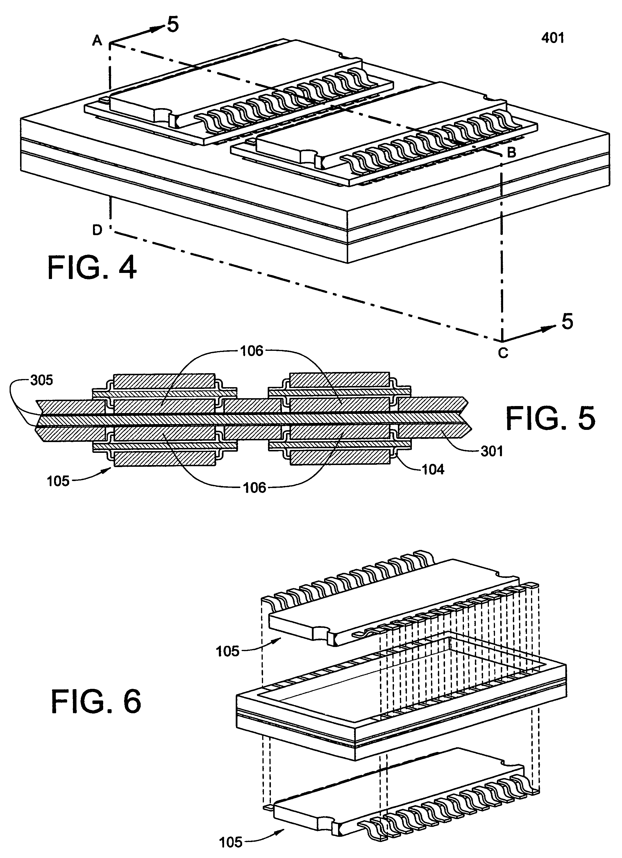
[0059]Referring now to FIG. 3, multiple first embodiment package units 201 (in this example, four) are shown ready for mounting on a circuit board 301. In this example, two package units 201A and 201B will be mounted on the upper surface 302U of the circuit board 301, while two package units 201C and 201D will be mounted on the lower surface 302L thereof. One IC package 105H of each package unit 201 fits within its own recess 303 in the circuit board 301 so that it is completely hidden from view, while the other IC package 105E is completely exposed. The surrounding edges of each recess are equipped with a set of board electrical connection contact pads 304. The leads of each hidden package 105H will make direct contact with the contact pads of its recess and will be routed within the circuit board 301 to the appropriate interconnection sites. The leads 104 of the exposed IC package 105E are coupled to the leads 104 of the connections which penetrate the laminar carrier 101. By usin...

second embodiment

[0063]Referring now to FIG. 9, surface mounting of the package units 701 on the circuit board 801 has resulted in a completed second embodiment module 901. A cross sectional view of the module 901 through the plane EFGH 902 provides the view of FIG. 10.

[0064]A third embodiment IC package unit, shown in FIGS. 11-14 is used for both third and fourth embodiment modules. The third embodiment package unit incorporates features of both the first and second embodiment package units 201 and 701, respectively. One of the pair of IC packages 105 is mounted on a planar surface of the carrier right-side up, while the other package is mounted within a recess on the opposite side of the carrier upside down. Using such a mounting configuration, both IC packages of each package unit are positioned as though stacked one on top of the other. For identical packages, interconnection of common signal lines is facilitated. Referring now to FIGS. 11-14, the third embodiment package unit utilizes a carrier...

third embodiment

[0066]Referring now to FIG. 16, surface mounting of the package units 1201 on the circuit board 1501 has resulted in a completed third embodiment module 1601. A cross sectional view of the module 1601 through the plane IJKL 1602 provides the view of FIG. 19.

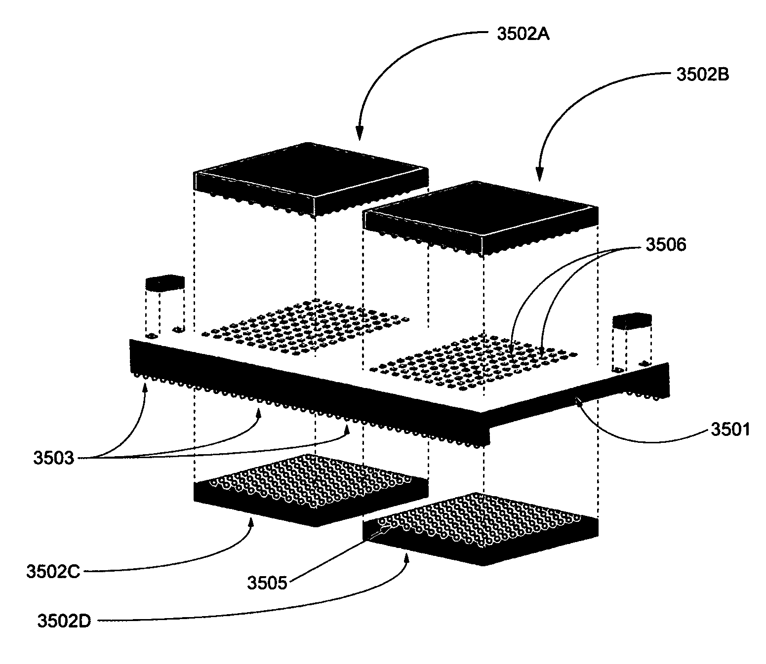
[0067]Referring now to FIG. 17, multiple third embodiment package units 1201 (in this example, four) are shown ready for mounting on a circuit board 1701 having two major opposing surfaces equipped with package unit mounting recesses 1702. In this example, two package units 1201A and 1201B will be mounted on the upper surface 1702U of a circuit board 1701, while two package units 1201C and 1201D will be mounted on the lower surface 1702L thereof. Each recessed mounting location on the circuit board 1701 has a set of board contact pads 1703 to which the leads 104 of a hidden adjacent IC package 105H of each package unit 1201A-1201D conductively bonded. The leads 104 of the exposed nonadjacent IC package 105E of each package unit 1...


PUM


Abstract

An improved multi-chip module includes a circuit board having an array of electrical interconnection pads to which are mounted a plurality of IC package units. Each IC package unit includes multiple IC packages, which are mounted on opposite sides of a package carrier. The package units may be mounted on one or both sides of the circuit board. A variety of package carriers are used to create a number of different modules. One type of package carrier has a pair of major planar surfaces. Each planar surface incorporates electrical contact pads. At least one IC package is surface mounted on each major planar surface, by interconnecting the connection elements, or leads, of the package with the contact pads on the planar surface, to form the IC package unit. Another type of package carrier substrate has a multiple recesses for back-to-back surface mounting of the IC packages. The package also includes in various versions heat sinks.

Description

[0001]This is a continuation of application Ser. No. 09 / 688 / 500 filed on Oct. 16, 2000 now U.S. Pat. No. 6,713,854.[0002]This invention is related to two U.S. patent applications, the first of which is application Ser. No. 09 / 285,354, which was filed on Apr. 2, 1999, and which is titled ELECTRONIC MODULE HAVING A THREE DIMENSIONAL ARRAY OF INTEGRATED CIRCUIT PACKAGES, the second of which is application Ser. No. 09 / 524,324, which was filed on Mar. 13, 2000, and which is titled ELECTRONIC MODULE HAVING A THREE DIMENSIONAL ARRAY OF INTEGRATED CIRCUIT PACKAGES.FIELD OF THE INVENTION[0003]This invention relates to the production of multi-chip electronic modules, and more particularly to a method and apparatus for attaching multiple integrated circuit packages to printed circuit boards. It also relates to high-density memory modules having three-dimensional arrangements of integrated circuit packages.BACKGROUND OF THE INVENTION[0004]Demand for semiconductor memory is highly elastic. When ...

Claims


Application Information

Patent Timeline
Patent Type & Authority Patents(United States)
IPC IPC(8): H01L23/02H01L25/18H01L25/10H01L25/11H05K1/14H05K1/18H05K3/34H05K3/36
CPCH05K1/141H05K1/182H05K3/3421H05K3/3442H05K3/368H05K2201/09072H01L2924/0002H05K2201/10689H05K2201/10734H05K2203/1572H01L2924/00H01L25/10
Inventor KLEDZIK, KENNETH J.ENGLE, JASON C.
Owner LEGACY ELECTRONICS INC
Why Eureka
Try Eureka