Solid state image pickup device and camera

a pickup device and solid-state image technology, applied in the direction of radio frequency controlled devices, instruments, television systems, etc., can solve the problem of not considering the capacitance of the above-described additional capacitors

Inactive Publication Date: 2008-08-05
CANON KK
View PDF42 Cites 115 Cited by
  • Summary
  • Abstract
  • Description
  • Claims
  • Application Information

AI Technical Summary

Problems solved by technology

However, in the above described conventional technology, the capacitance of the above described additional capacitor is not concretely considered.

Method used


Image

  • Solid state image pickup device and camera
  • Solid state image pickup device and camera
  • Solid state image pickup device and camera

Examples


first embodiment

[0027]In the next place, a first embodiment according to the present invention will be described with reference to the drawings.

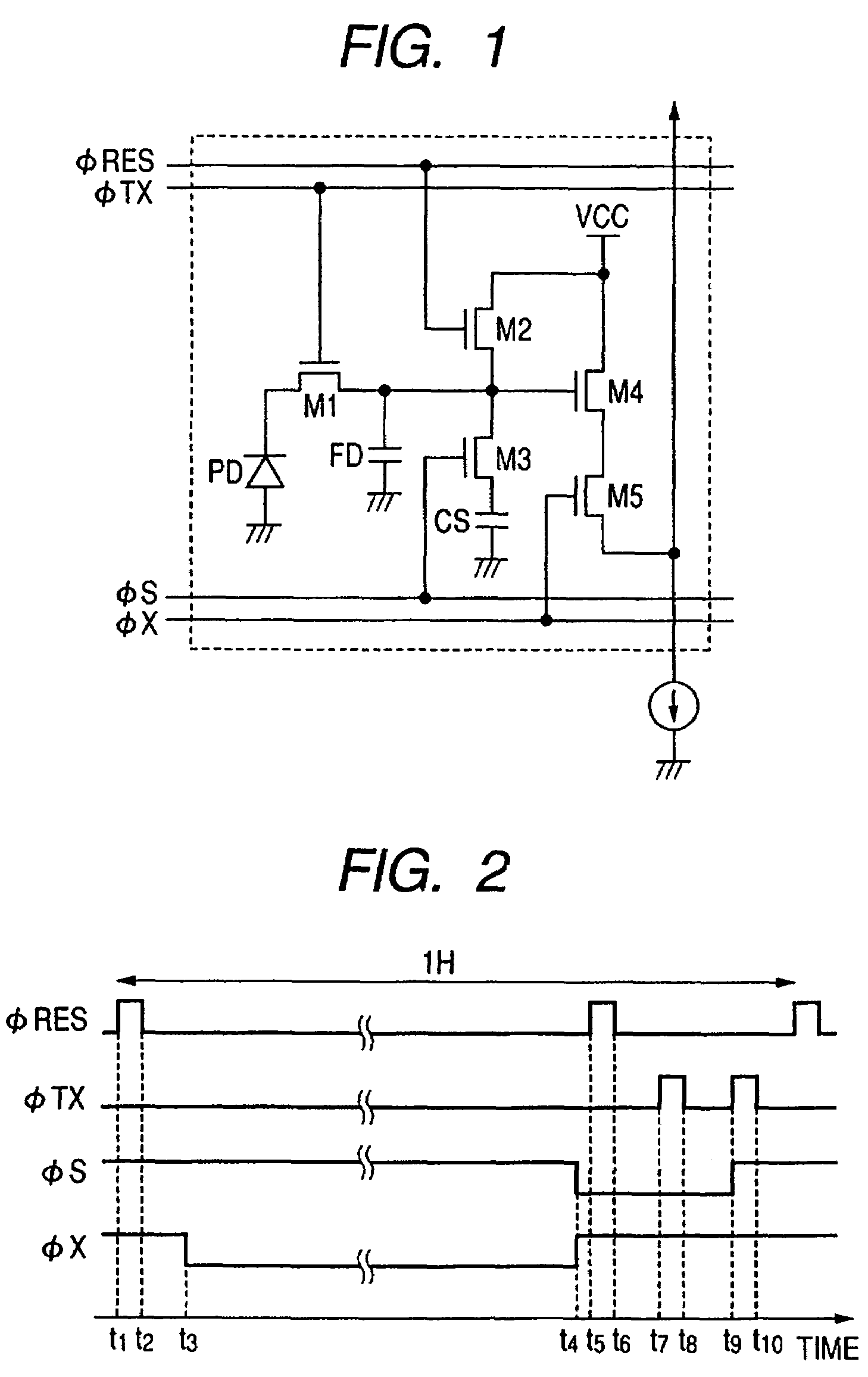
[0028]FIG. 1 is a view showing an example of a diagrammatic configuration of a pixel provided in a solid state image pickup device of the present embodiment.

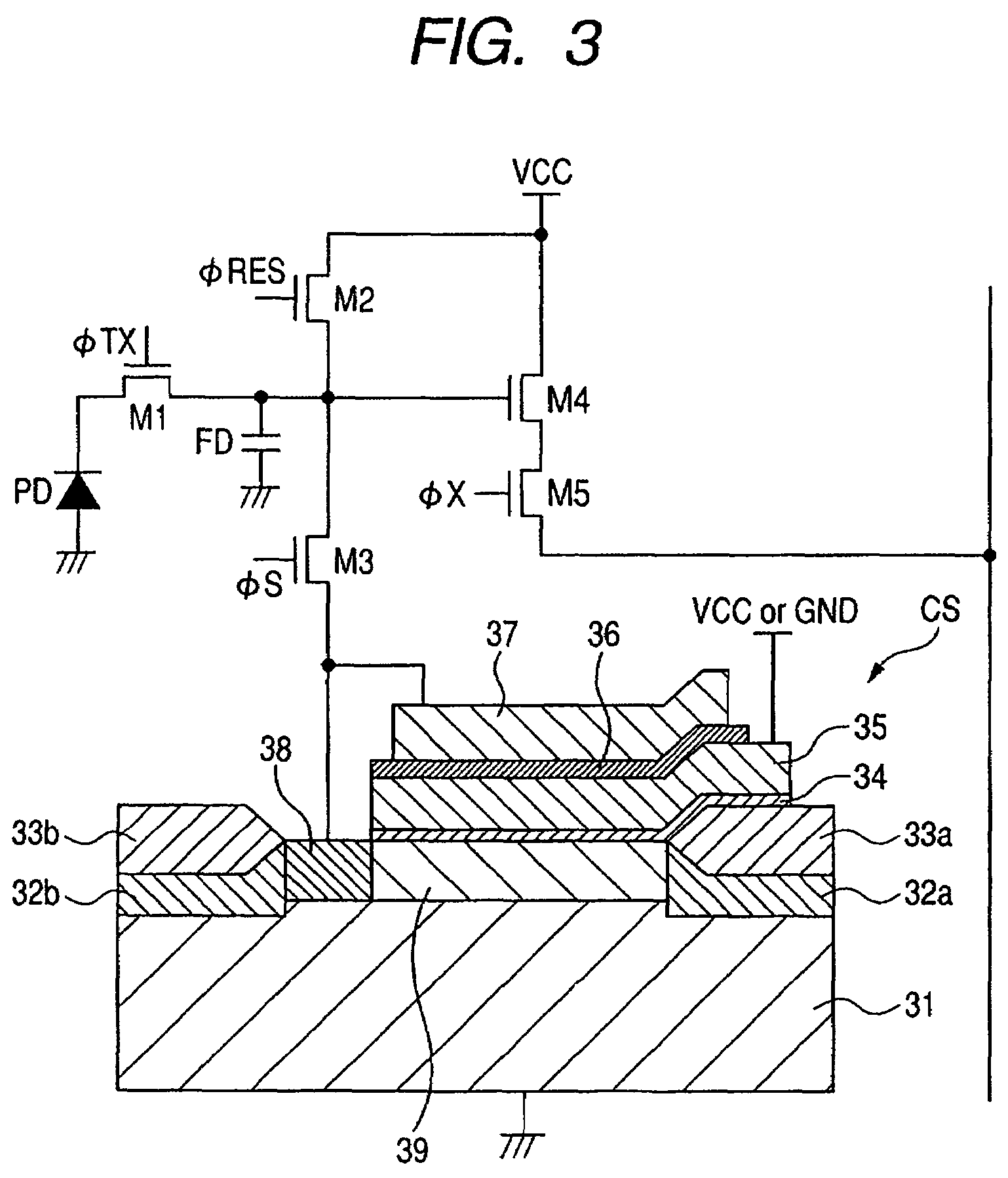
[0029]In FIG. 1, the solid state image pickup device of the present embodiment contains the pixel having a photodiode PD, a first transfer MOS transistor M1, a reset MOS transistor M2, a second transfer MOS transistor M3, a source follower MOS transistor M4, and a selective MOS transistor M5; and has a plurality of the pixels configured into a two-dimensional matrix consisting of n lines and m rows (in which n and m are natural numbers).

[0030]A photodiode PD is connected to a floating diffusion region FD through a first transfer MOS transistor M1. A source or a drain region of a reset MOS transistor M2 is connected to the floating diffusion region FD. A gate of the source follower MOS transistor M4 is a...

second embodiment

[0065]In the next place, a second embodiment according to the present invention will be described. The present embodiment differs from the first embodiment only in a connecting method of an additional capacitor CS. For this reason, the same parts as in the first embodiment are marked with the same reference numerals as those marked in FIGS. 1, 2 and 3, and the detailed description on them will be omitted.

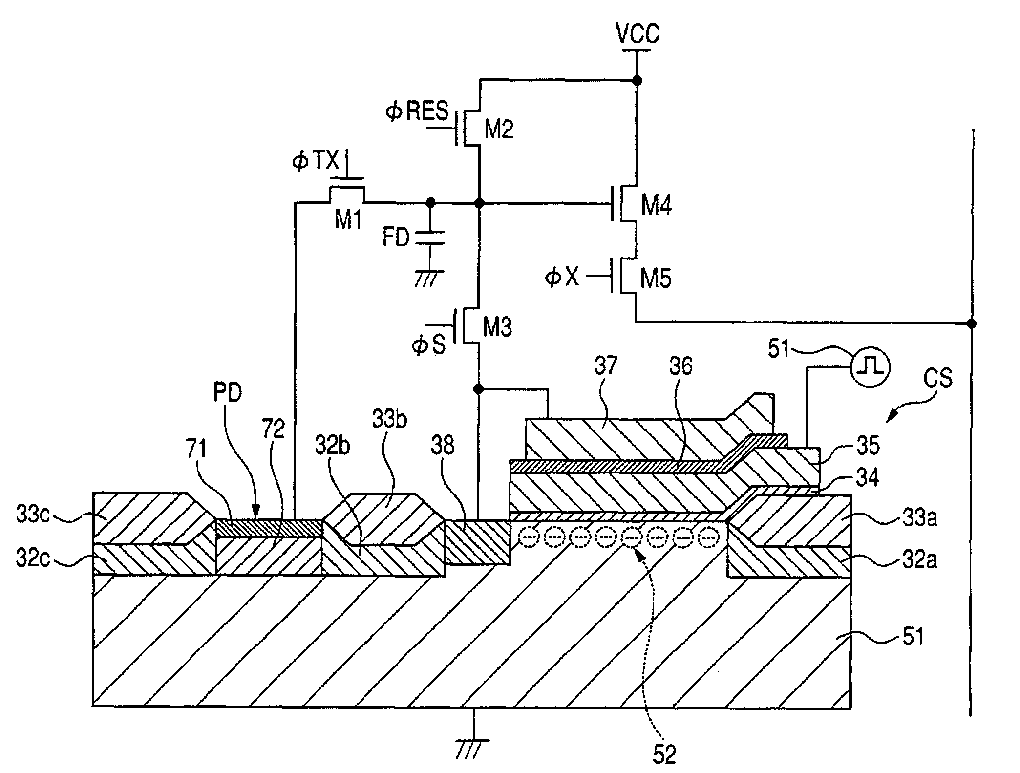
[0066]FIG. 4 is a sectional side view showing one example for the configuration of an additional capacitor CS in the present embodiment; and also shows a connected state of the additional capacitor CS in the pixel shown in FIG. 1.

[0067]As is shown in FIG. 4, in the present embodiment, a second diffusion layer 39 is connected to a ground potential GND, a second polysilicon layer 37 is connected to a power supply potential Vcc or a ground potential GND, and a first polysilicon layer 35 is connected to a second transfer MOS transistor M3. Thus, the solid state image pickup device in th...

third embodiment

[0070]In the next place, a third embodiment according to the present invention will be described. The present embodiment differs from the first embodiment only in the configuration and a part of a connecting method of an additional capacitor CS. For this reason, the same parts as in the first embodiment are marked with the same reference numerals as those marked in FIGS. 1, 2 and 3, and the detailed description on them will be omitted.

[0071]FIG. 5 is a sectional side view showing one example for the configuration of an additional capacitor CS in the present embodiment; and also shows a connected state of the additional capacitor CS in the pixel shown in FIG. 1.

[0072]As is shown in FIG. 5, an additional capacitor CS in the present embodiment has a configuration in which a second diffusion layer 39 is removed from a capacitor CS in the first embodiment. Though a first polysilicon layer 35 in the capacitor CS of the first embodiment is connected to a power supply potential Vcc or a gro...


PUM


Abstract

An object of the present invention is to simultaneously realize the enlargement of a dynamic range and the downsizing of a pixel. An additional capacitor CS is composed by using: a first capacitor formed of a first diffusion layer, a second diffusion layer and a P well by layering the P well, the first diffusion layer, a first dielectric film, a first polysilicon layer, a second dielectric film and a second polysilicon layer; a second capacitor formed of the second diffusion layer, the first polysilicon layer and the first dielectric film; and a third capacitor formed of the first polysilicon layers, a second polysilicon layer, and a second dielectric film. Thereby, the additional capacitor CS for accumulating carriers overflown from a photodiode PD can secure a required capacitance value while making its size as small as possible.

Description

BACKGROUND OF THE INVENTION[0001]1. Field of the Invention[0002]The present invention relates to a solid state image pickup device and to a camera, and particularly to those suitably used in a CMOS area sensor.[0003]2. Related Background Art[0004]In recent years, a CMOS area sensor having a photodiode and a MOS transistor integrated into one-chip has been used for a solid-state image sensing device. The CMOS area sensor has advantages of consuming a less electric power, needing a lower drive power and working in a higher speed than a CCD. Accordingly, the CMOS area sensor is expected to grow in demand in future.[0005]For this reason, it has been proposed to enlarge a dynamic range of a solid-state image sensing device, by using such a CMOS area sensor.[0006]The solid-state image sensing device includes a plurality of pixels having, for instance; a photodiode; a floating diffusion region (which may be abbreviated as FD, hereafter as needed); a first transfer transistor for transferri...

Claims


Application Information

Patent Timeline
Patent Type & Authority Patents(United States)
IPC IPC(8): H01L31/058H01L27/146H04N5/335H04N5/355H04N5/369H04N5/374H04N5/376
CPCH01L27/14625H01L27/14632H04N5/37452H04N3/155H04N5/3559H01L27/14656H04N25/59H04N25/771
Inventor OGURA, MASANORIKOIZUMI, TORUOKITA, AKIRAITANO, TETSUYAKIKUCHI, SHIN
Owner CANON KK
Why Eureka
Try Eureka