
System and method for testing circuitry on a wafer

Active Publication Date: 2008-08-12
ADVANTEST CORP
View PDF25 Cites 27 Cited by
  • Summary
  • Abstract
  • Description
  • Claims
  • Application Information

AI Technical Summary

Benefits of technology

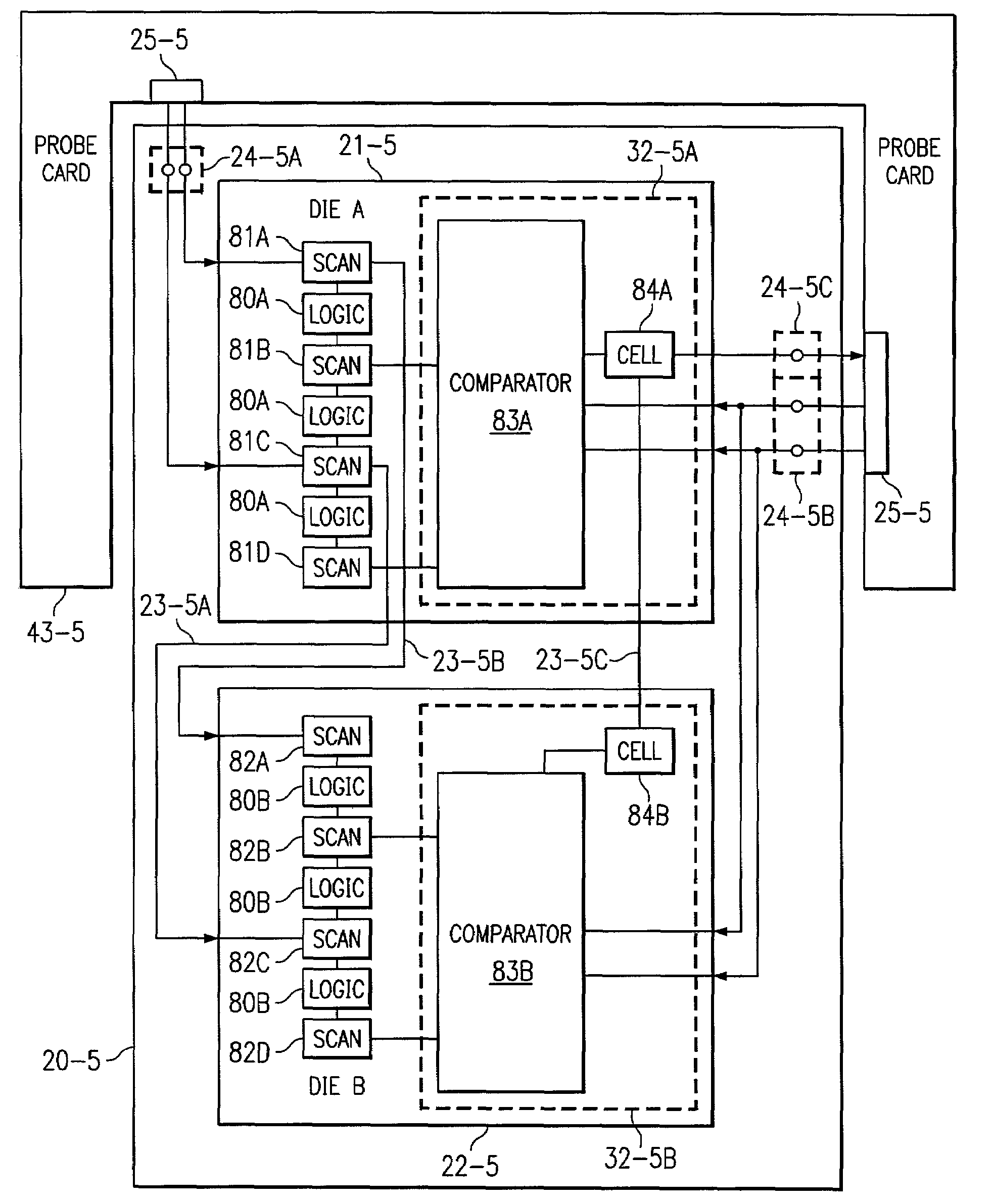
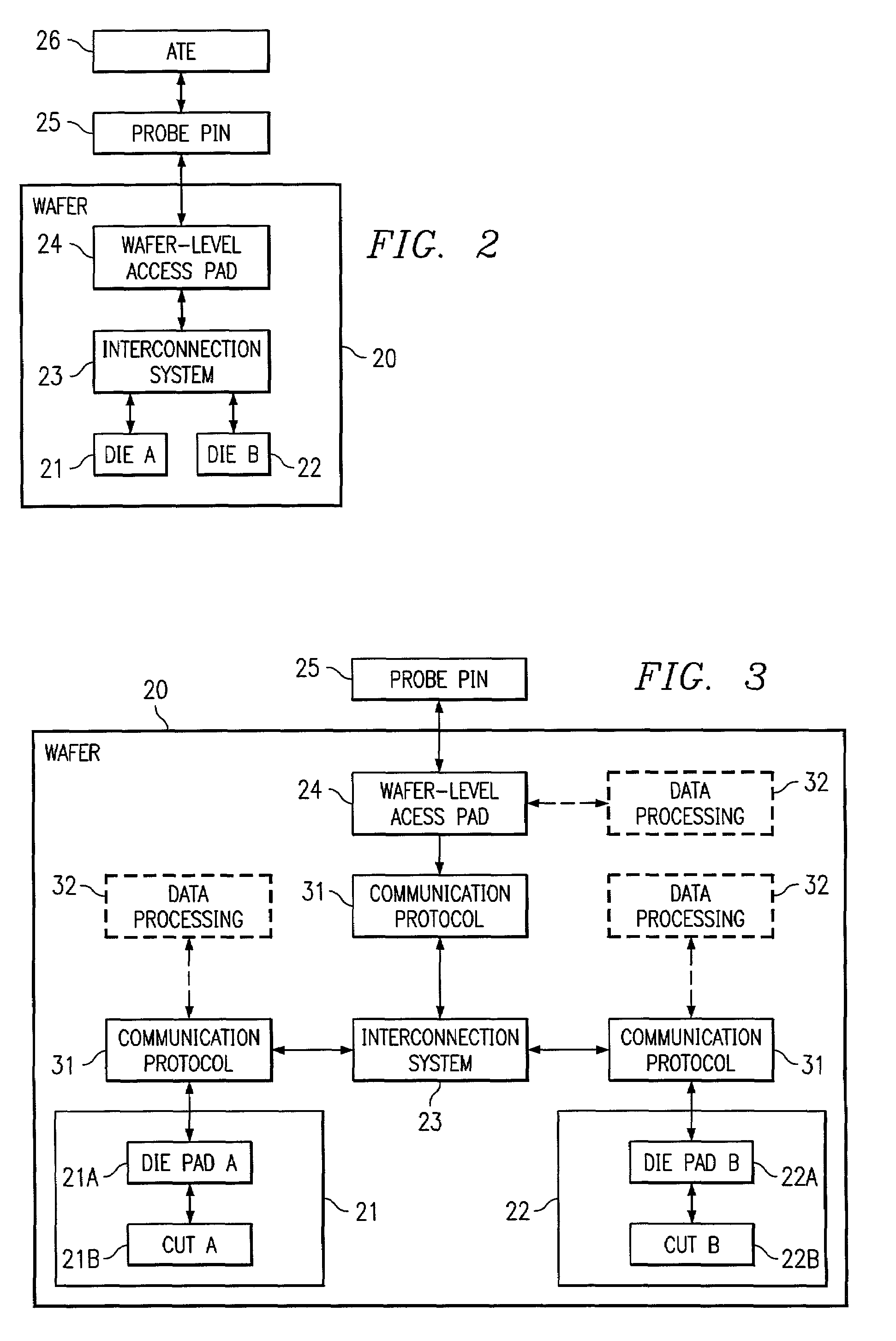
[0015]The present invention is directed to a system and method in which a plurality of dice on a semiconductor wafer are interconnected in a manner that enables efficient testing thereof. For example, in certain embodiments a plurality of dice are interconnected in a manner that enables test data to be communicated from a tester system, which may be external to the semiconductor wafer (e.g., via a test probe) or which may be implemented on the semiconductor wafer (e.g., as Built-In Self Test circuitry), to a plurality of dice for concurrent testing of such plurality of dice. Depending on the amount of interconnection, all or a portion of each of the plurality of dice may be tested concurrently. For example, in certain implementations test data may be communicated to a first die, and a second die may be interconnected to the first die such that all or a portion of such second die is tested concurrently with the first die.
[0016]In certain embodiments of the present invention, a plurality of dice are interconnected in a manner that enables test data to be communicated from one die to at least one other die. Thus, for example, input and / or output test data may be communicated from at least one die to at least one other die. In certain embodiments of the present invention, a plurality of dice are interconnected in a manner that enables such dice to be tested concurrently while maintaining a repeatable pattern at the reticle level for fabricating such dice.
[0019]Accordingly various embodiments of the present invention may provide several technological advantages. As one example, certain embodiments provide a test scheme that enables multiple dice on a wafer to be tested concurrently while maintaining regularity at the wafer level (i.e., a repeatable pattern at the reticle level). As another example, certain embodiments provide a test scheme in which a plurality of dice on a wafer are communicatively interconnected such that test data may be communicated from at least one die to at least one other die. As a further example, certain embodiments of the present invention provide a test scheme that provides great efficiency in testing dice because, for instance, multiple dice (or at least portions thereof) may be tested concurrently (thereby reducing the overall amount of time required for testing the dice of a wafer).
[0020]Also, certain embodiments of the present invention provide a test scheme that provides improved utilization of test resources, such as a test probe. For instance, considering that some test resources, such as a test probe, are relatively expensive, it is often desirable to obtain maximum utilization of such resources. Certain embodiments of the present invention enable improved utilization of resources, such as a test probe. Additionally, certain embodiments of the present invention provide efficient utilization of wafer and / or dice area for implementing a dice testing scheme. For example, certain embodiments may share area on a plurality of dice to implement a test scheme for such dice. For instance, certain embodiments may implement a test scheme (e.g., BIST circuitry) with portions of such test scheme distributed on various different dice. Further, certain embodiments of the present invention provide a test scheme that enables one die to test one or more other dice of a wafer. Accordingly, such test schemes may provide for improved signal integrity in testing dice on a wafer because, for instance, the tester circuitry is in close proximity to the dice logic being tested. Additionally, the same technologies are preferably used for implementing the test circuitry and / or communication scheme interconnecting a plurality of dice as is used for implementing the dice logic, which may improve the scalability and signal integrity of embodiments of the present invention. Further, certain embodiments of the present invention may be used to implement loop back testing.

Problems solved by technology

In most testing procedures, each die is probed using very costly probe equipment while the dice are still on the wafer.
That is, if it is determined that a detected defect cannot be repaired, the time and expense of completing a chip assembly will not be expended.
Traditional testing procedures are problematic because of their serial nature.
For example, using a probe to test one die after another die results in an undesirably long time being required for testing all of the dice of a wafer, which effectively increases the overall cost of testing the dice.
Probes used for testing the dice are generally very expensive, and it is therefore undesirable to have a probe tied up for a long time testing each die.
Additionally, while certain probe implementations may provide a sufficient number of pins to enable a plurality of dice to be tested simultaneously, such testing is limited by the configuration (e.g., the number of pins) of the probe.
For instance, a probe that comprises sufficient pins for contacting two dice simultaneously is limited to testing of two dice concurrently.
Thus, if it is desired to test four dice, the probe configuration is incapable of testing all four dice simultaneously.
Thus, generally the communication to the dice for testing is limited by the probe card's configuration.
In addition, physical constraints may limit the amount of parallelism that may be achieved through modifying a probe's configuration (e.g., to include more pins).
For example, in some instances it may not be technologically possible to arrange the pins of a probe in a manner (e.g., sufficiently close together) to enable testing of a desired number of dice, or implementing such an arrangement may not be cost effective.
Traditional testing procedures that require a probe to touch down on one (or a few) dice at a time effectively increases the wear of a probe.
While parallel testing solutions of the prior art propose communicatively coupling a wafer-level access pad to multiple dice to enable data to be communicated from the access pad to the dice in parallel (and vice-versa), such solutions do not provide a communication scheme for improving / optimizing efficiency and reliability of the testing.
Further, parallel testing solutions proposed in the prior art are difficult and / or not cost effective to manufacture.
However, this measurement cannot be used to point to certain defects on dies in isolation.
Semiconductor manufacturers spend a significant amount of money packaging defective dice which pass the testing performed during probing, but which do not pass the reliability testing after packaging.
For multi-chip modules, it is quite costly to replace one or more failed dice once the dice have been bonded onto a substrate.
In addition, many manufacturers of multi-chip modules are requiring that semiconductor manufacturers sell them fully tested “known good dice” that have passed reliability tests and that are not packaged in an integrated circuit package.

Method used


Image

  • System and method for testing circuitry on a wafer
  • System and method for testing circuitry on a wafer
  • System and method for testing circuitry on a wafer

Examples


Embodiment Construction

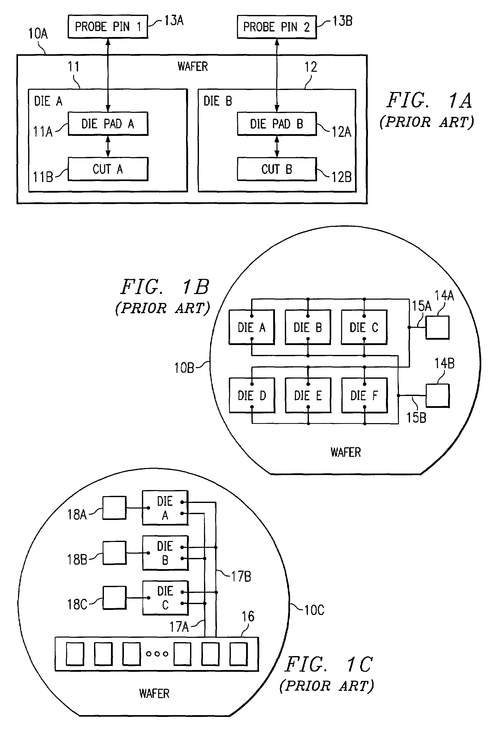
[0036]Turning to FIGS. 1A-1C, example configurations of the existing art for testing dice of a semiconductor wafer are shown. FIG. 1A shows an example of a traditional testing configuration. As shown, wafer 10A comprises die A (labeled 11 in FIG. 1A) and die B (labeled 12 in FIG. 1A), which may be singulated during the singulation process (e.g., and may be packaged as an integrated circuit). Of course, wafer 10A may comprise many more than two dice, but only two are shown in FIG. 1A for simplicity. Die A includes circuitry (“CUT A”) 11B, and die B likewise includes circuitry (“CUT B”) 12B. Such circuitry may be referred to herein as the CUT of a die. Such circuitry 11B and 12B of dice A and B are typically identical, but in some manufacturing processes, differing circuitry may be included at different dice of a wafer.

[0037]Die A also includes one or more access pads 11A that are communicatively coupled to circuitry 11B, and die B likewise includes one or more access pads 12A that ar...


PUM


Abstract

A system and method in which a plurality of dice on a semiconductor wafer are interconnected to enable efficient testing thereof. In certain embodiments a plurality of dice are interconnected in a manner that enables test data to be communicated from a tester system to a plurality of dice for concurrent testing of such plurality of dice. Depending on the amount of interconnection, all or a portion of each of the plurality of dice may be tested concurrently. In certain embodiments, a plurality of dice are interconnected in a manner that enables test data to be communicated from one die to at least one other die. In certain embodiments, a plurality of dice are interconnected in a manner that enables such dice to be tested concurrently while maintaining a repeatable pattern at the reticle level for fabricating such dice.

Description

TECHNICAL FIELD[0001]The present invention relates in general to testing of circuitry on a semiconductor wafer, and more particularly to a system and method for wafer-level testing of circuitry utilizing communicative interconnection between dies on the wafer.BACKGROUND OF THE INVENTION[0002]During typical semiconductor manufacturing processes, a plurality of integrated circuits are formed as individual dice on a semiconductor wafer. Each semiconductor wafer generally has dozens to hundreds of individual dice formed thereon. Once the dice are formed on a semiconductor wafer, the dice are then tested to determine which dice are functional and which dice are not functional. In most testing procedures, each die is probed using very costly probe equipment while the dice are still on the wafer. This step is also known as “wafer sort.”[0003]The purpose of the wafer-level probe test is to determine, as early as possible in the manufacturing process, whether each individual die is defective...

Claims


Application Information

Patent Timeline
IPC IPC(8): G01R31/28G01R31/3185H01L21/66
CPCG01R31/318511G01R31/318505G01R31/2884G01R31/318533
Inventor VOLKERINK, ERIK H.KOCHE, AJAY
Owner ADVANTEST CORP
Learn More