Acceleration sensor and method for manufacturing the same

a sensor and acceleration technology, applied in the field of acceleration sensors, can solve the problem of longer side-etching process tim

Inactive Publication Date: 2008-09-02
DENSO CORP
View PDF13 Cites 25 Cited by
  • Summary
  • Abstract
  • Description
  • Claims
  • Application Information

AI Technical Summary

Benefits of technology

[0017]Accordingly, since the side-etching process is controlled with respect to the widths of the movable and fixed electrodes, the thicknesses of the movable and the fixed electrodes are controlled with small deviation. Thus, the deviation of thickness is improved. Further, manufacturing quality of the sensor is improved.
[0027]Accordingly, since the side-etching process is controlled with respect to the widths of the movable and fixed electrodes, the thicknesses of the movable and the fixed electrodes are controlled with small deviation. Thus, the deviation of thickness is improved. Further, manufacturing quality of the sensor is improved.

Problems solved by technology

On the other hand, when the width of the movable electrode is wide, the side-etching process time becomes longer.

Method used


Image

  • Acceleration sensor and method for manufacturing the same
  • Acceleration sensor and method for manufacturing the same
  • Acceleration sensor and method for manufacturing the same

Examples


first embodiment

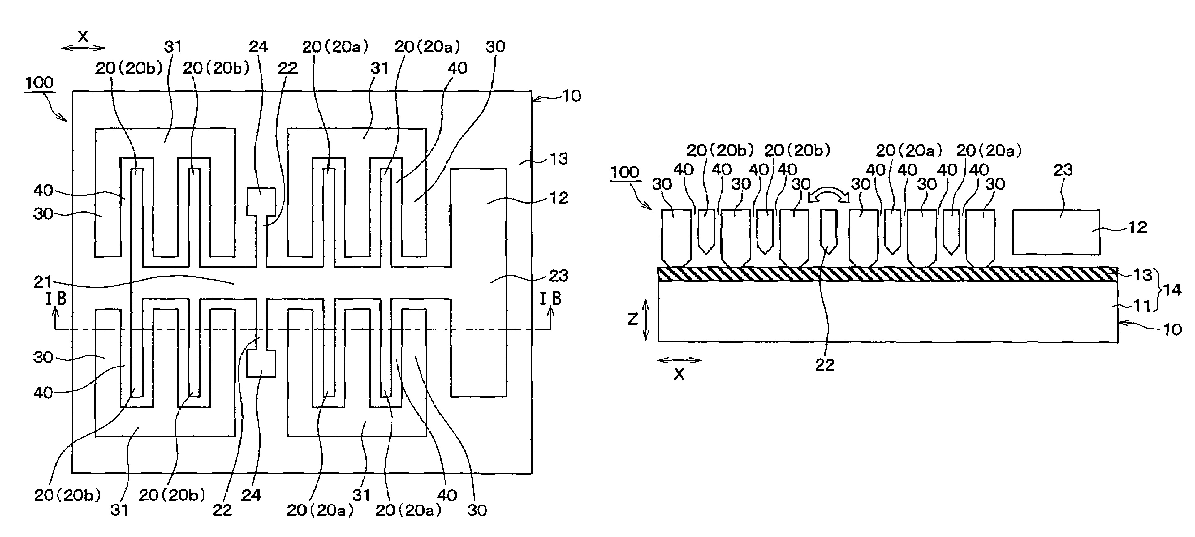
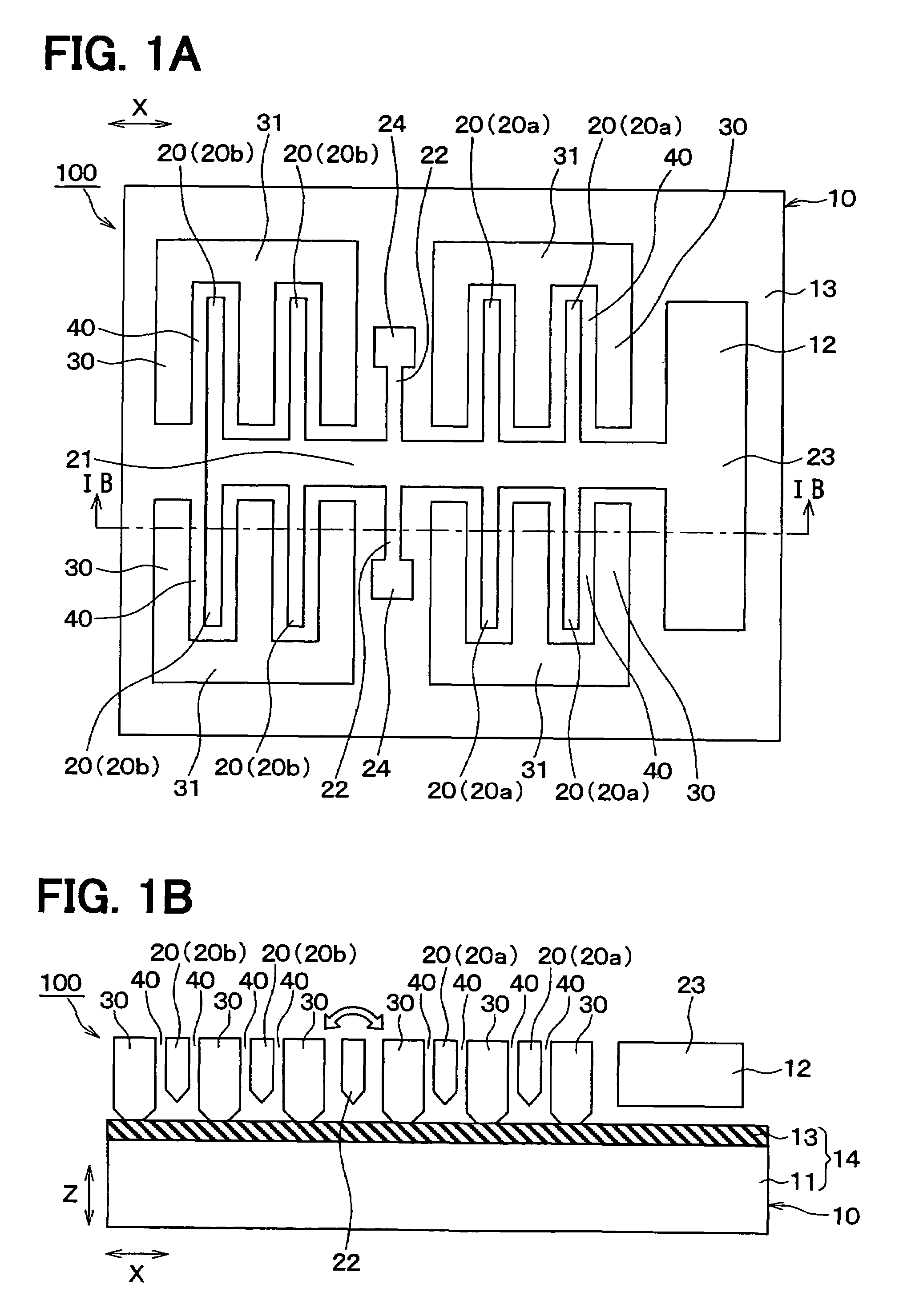
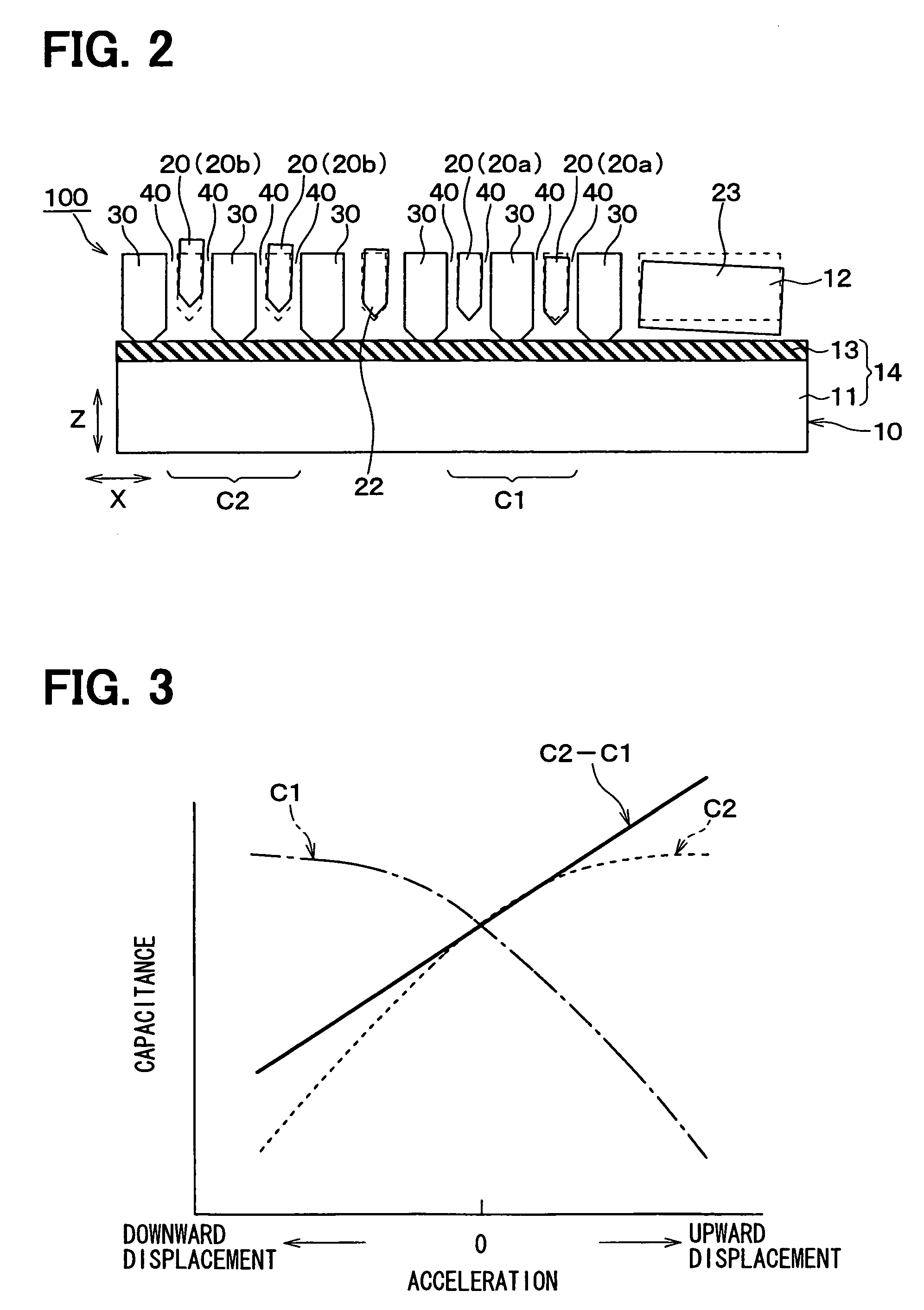
[0040]FIGS. 1A and 1B are diagrams for schematically showing a structure of an acceleration sensor 100 according to a first embodiment of the present invention. Concretely speaking, FIG. 1A is a plan view for schematically indicating the acceleration sensor 100, FIG. 1B is a sectional view for schematically indicating the acceleration sensor 100, taken along a dot / dash line IB-IB FIG. 1A.

[0041](Structure)

[0042]As represented in FIG. 1B, the acceleration sensor 100 is provided with a semiconductor substrate 10. The semiconductor substrate 10 is made by stacking a silicon semiconductor layer 12 on a supporting substrate 14.

[0043]In this first embodiment, the semiconductor substrate 10 has been manufactured as an SOI (silicon-on-insulator) substrate 10 made by stacking a second silicon semiconductor layer 12 via an insulating layer 13 on a first silicon semiconductor layer 11.

[0044]Then, in this semiconductor substrate 10, while both the first silicon semiconductor layer 11 and the ins...

second embodiment

[0153]FIGS. 8A and 8B are diagrams for schematically showing a structure of an acceleration sensor 200 according to a second embodiment of the present invention. Concretely speaking, FIG. 8A is a plan view for schematically showing the acceleration sensor 200, and FIG. 8B is a sectional view for schematically indicating the acceleration sensor 200, taken along a dot / dash line VIIIB-VIIIB of FIG. 8A.

[0154]As shown in FIGS. 8A and 8B, similarly, the acceleration sensor 200 according to this second embodiment is featured by having the below-mentioned basic structure. That is to say, a vertical displacement type acceleration sensor corresponding to this acceleration sensor 200 is provided with a semiconductor substrate 10 made by stacking a silicon semiconductor layer 12 on a supporting substrate 14; a trench etching process operation is carried out with respect to the silicon semiconductor layer 12 along a first direction “Z”, so that both a movable electrode 20 and a fixed electrode 3...


PUM


Abstract

An acceleration sensor includes: a semiconductor substrate including a support layer and a semiconductor layer, which are stacked in a first direction; a movable electrode and a fixed electrode; and a trench. The movable electrode separately faces the fixed electrode by sandwiching the trench along with a second direction. The trench has a detection distance in the second direction. The movable electrode is movable along with the first direction when acceleration is applied. The movable electrode has a bottom apart from the support layer. The width of the movable electrode along with the second direction is smaller than the width of the fixed electrode. The thickness of the movable electrode along with the first direction is smaller than the thickness of the fixed electrode.

Description

CROSS REFERENCE TO RELATED APPLICATION[0001]This application is based on Japanese Patent Application No. 2005-85405 filed on Mar. 24, 2005, the disclosure of which is incorporated herein by reference.FIELD OF THE INVENTION[0002]The present invention relates to an acceleration sensor and a method for manufacturing an acceleration sensor.BACKGROUND OF THE INVENTION[0003]Conventionally, as this sort of acceleration sensors, such an acceleration sensor has been proposed in, for example, JP-A-2003-14778, which corresponds to U.S. Pat. No. 6,739,189-B2. That is, while a semiconductor substrate made by stacking a silicon semiconductor layer on a supporting substrate is prepared, since a trench etching process operation is carried out along a first direction (namely, a vertical direction of substrate plane) perpendicular to a substrate plane of the semiconductor substrate with respect to the silicon semiconductor layer, both a movable electrode and a fixed electrode are patterned and formed...

Claims


Application Information

Patent Timeline
Patent Type & Authority Patents(United States)
IPC IPC(8): G01P15/125G01P15/00
CPCB81B3/0086G01P15/125G01P15/0802B81B2201/0235G01P2015/0831
Inventor ASAMI, KAZUSHITAKEUCHI, YUKIHIROYOKOYAMA, KENICHI
Owner DENSO CORP
Why Eureka
Try Eureka