Capacitor element

a technology of capacitors and elements, applied in capacitors, solid-state devices, transistors, etc., can solve the problems of difficult to reduce level differences, difficult to obtain focus margins in a range, and difficult to commercialize high-performance and high-integration semiconductor memory devices. achieve the effect of small area, simple and easy method, and large capacitan

Active Publication Date: 2008-09-02
GK BRIDGE 1
View PDF12 Cites 15 Cited by
  • Summary
  • Abstract
  • Description
  • Claims
  • Application Information

AI Technical Summary

Benefits of technology

[0030]In the capacitor element having the planar structure used in the first conventional embodiment, the height of the capacitor element is extremely small. This allows easy obtention of a focus margin in a range achievable with the performance of a stepper in a lithographic step during wiring formation, which is performed after the formation of the capacitor elements, even after the formation of the structure in which the capacitor element is covered completely with the hydrogen barrier films. This also allows easy obtention of a focus margin in a range achievable with the performance of a stepper in a lithographic step performed to form a mask pattern when the hydrogen barrier film disposed over the capacitor element and connected to the hydrogen barrier film disposed thereunder is processed.
[0122]In the second method for fabricating a capacitor element, the step of forming the first hydrogen barrier film may appropriately include forming a hydrogen barrier material over the sidewall and bottom portion of the hole and the upper surface of the interlayer insulating film and then selectively removing the hydrogen barrier material formed on the upper surface of the interlayer insulating film by CMP or an etch-back process. This allows the formation of a hydrogen barrier film having a cylindrical configuration using a simple and easy method.

Problems solved by technology

However, because a structure in which a capacitor element composed of a three-dimensional structure using a ferroelectric or high dielectric material for a capacitor dielectric film is covered completely with a hydrogen barrier film cannot easily be implemented by using the conventional capacitor elements described above, a high-performance and high-integration semiconductor memory device cannot be commercialized.
In the capacitor element having the projecting three-dimensional structure used in the second conventional embodiment, however, the capacitor element is required to have a height of about 1 μm so that it is extremely difficult to reduce the level difference resulting from the height of the capacitor element over the entire surface of a wafer.
Accordingly, it becomes extremely difficult to obtain a focus margin in a range achievable with the performance of a stepper in a lithographic step during wiring formation performed after the formation of the capacitor elements.
It also becomes extremely difficult to obtain a focus margin in a range achievable with the performance of a stepper in a lithographic step performed to form a mask pattern when the hydrogen barrier film disposed over the capacitor element and connected to the hydrogen barrier film disposed thereunder is processed.

Method used


Image

  • Capacitor element
  • Capacitor element
  • Capacitor element

Examples


embodiment 1

Variation 4 of Embodiment 1

[0181]A capacitor element according to a fourth variation of the first embodiment will be described herein below with reference to FIGS. 7A, 7B, 8A, and 8B.

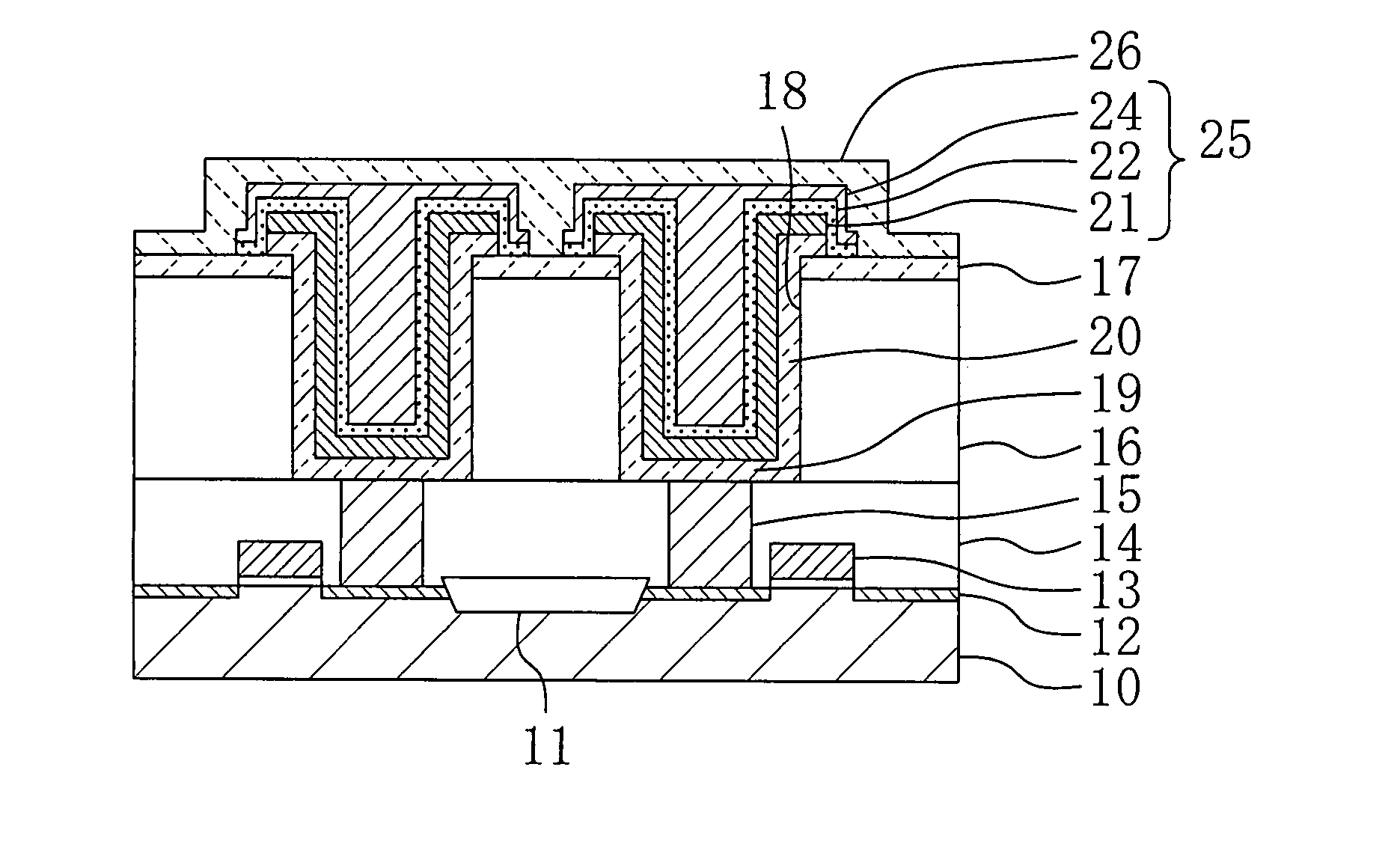
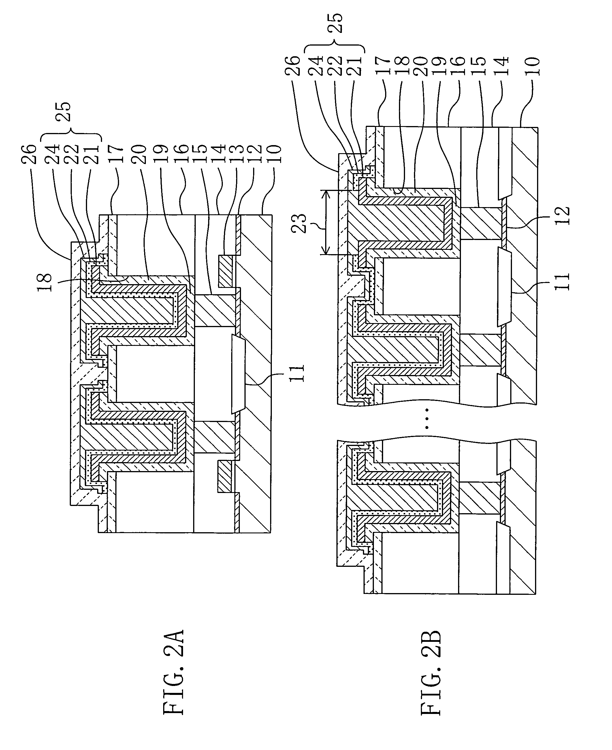
[0182]FIGS. 7A, 7B, 8A, and 8B show principal-portion cross-sectional views of the capacitor element according to the fourth variation of the first embodiment. The same reference numerals will be retained for those of the components shown in FIGS. 7A, 7B, 8A, and 8B which are common to the components shown in FIGS. 2A, 2B, 3, 4, 5A, 5B, 6A, and 6B and the description thereof will not be repeated.

[0183]Because the characteristic portion of the capacitor element according to the fourth variation is that seventh hydrogen barrier films 29 are disposed, the description will be given mainly to the characteristic portion herein below.

[0184]First, the structure of the capacitor element according to the fourth variation shown in FIG. 7A is greatly different from the structure shown in FIG. 5A in that the seventh...

embodiment 2

Variation 4 of Embodiment 2

[0236]A method for fabricating the capacitor element according to a fourth variation of the second embodiment will be described herein below with reference to FIGS. 7A, 7B, 8A, 8B, 9A to 9C, 10A, and 10B. The method for fabricating the capacitor element according to the fourth variation of the second embodiment is a method for fabricating the capacitor element shown in FIGS. 7A, 7B, 8A, and 8B. In contrast to the first to third variations described above, the fourth variation is characterized in that the seventh hydrogen barrier films 29 are disposed so that the description will be given mainly to a method for disposing the seventh hydrogen barrier films 29 herein below.

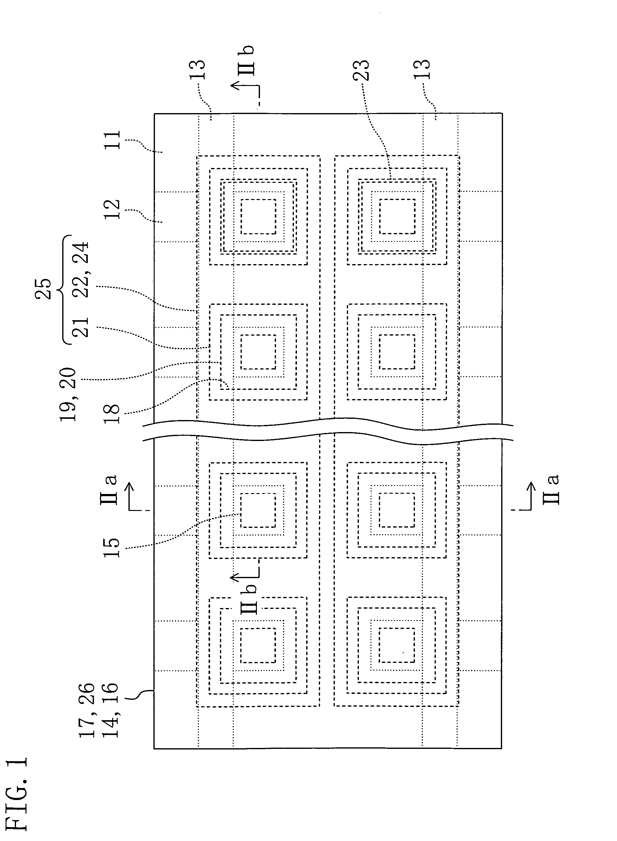
[0237]As shown in FIGS. 7A, 7B, 8A, and 8B, the isolation region 11 and the active regions 12 are formed on the semiconductor substrate 10 and the gates 13 are further formed thereon.

[0238]Next, SiO2 or SiN is deposited to cover the entire surface of the semiconductor substrate 10 by CVD an...

embodiment 3

Variation 4 of Embodiment 3

[0283]A capacitor element according to a fourth variation of the third embodiment will be described herein below with reference to FIGS. 16A, 16B, 17A, and 17B.

[0284]FIGS. 16A, 16B, 17A, and 17B show principal-portion cross-sectional views of the capacitor element according to the fourth variation of the third embodiment. The same reference numerals will be retained for those of the components shown inFIGS. 16A, 16B, 17A, and 17B which are common to the components shown in FIGS. 12A, 12B, 13A, 13B, 14A, 14B, 15A, and 15B and the description thereof will not be repeated.

[0285]Because the characteristic portion of the capacitor element according to the fourth variation is that seventh hydrogen barrier films 69 are disposed, the description will be given mainly to the characteristic portion herein below.

[0286]First, the structure of the capacitor element according to the fourth variation shown in FIG. 16A is greatly different from the structure shown in FIG. ...


PUM


Abstract

A capacitor element is provided which is composed of a lower electrode, an upper electrode formed in opposing relation to the lower electrode, and a capacitor dielectric film made of a ferroelectric material or a high dielectric material and formed between the lower and upper electrodes. The lower electrode, the capacitor dielectric film, and the upper electrode are formed in a region extending at least from within a hole provided in an interlayer insulating film having a first hydrogen barrier film disposed on the upper surface thereof toward a position above the hole. A second hydrogen barrier film in contact with the first hydrogen barrier film is disposed to cover the upper surface of the upper electrode and the side surface of the portion of the upper electrode which has been formed above the hole.

Description

CROSS-REFERENCE TO RELATED APPLICATIONS[0001]This application claims priority under 35 U.S.C. §119 on Patent Application No. 2004-022043 filed in Japan on Jan. 29, 2004, the entire contents of which are hereby incorporated by reference.BACKGROUND OF THE INVENTION[0002]The present invention relates to a capacitor element having a three-dimensional structure and using a capacitor dielectric film made of a ferroelectric material or a high dielectric material.[0003]To commercialize a RAM which enables high-speed wiring and reading at an unprecedentedly low voltage, vigorous research and development has been made on a ferroelectric material having a characteristic of spontaneous polarization or a high dielectric material. To implement a megabit-class semiconductor memory device to be mounted on an LSI composed of a CMOS with design rules of 0.18 μm or below, in particular, a capacitor element having a three-dimensional structure capable of providing a large capacitance with a small area ...

Claims


Application Information

Patent Timeline
Patent Type & Authority Patents(United States)
IPC IPC(8): H01L31/062H01L27/108H01L31/113H01L29/76H01L29/94H01L27/04H01L21/02H01L21/822H01L21/8239H01L21/8242H01L21/8246H01L27/10H01L27/105H01L27/11507H01L29/00
CPCH01L28/65H01L28/57H01L27/10852H01L28/75H10B12/033
Inventor NAGANO, YOSHIHISAMIKAWA, TAKUMI
Owner GK BRIDGE 1
Why Eureka
Try Eureka