Device and driving method thereof

a technology of a display device and a driving method, applied in the field of display devices, can solve the problems of insufficient practical period to write in, slow speed to write in, and difficulty in obtaining the period to write a video signal in a pixel, so as to increase the size of a display device and enhance the definition

Inactive Publication Date: 2008-09-16
SEMICON ENERGY LAB CO LTD
View PDF54 Cites 54 Cited by
  • Summary
  • Abstract
  • Description
  • Claims
  • Application Information

AI Technical Summary

Benefits of technology

[0010]The present invention has been made in view of the above problems. It is an object of the present invention to provide a display device and its driving method free from lack of writing time, which usually accompanies an increase in size of a display device and enhancement in definition. More particularly, a further object of the present invention is to provide a display device and its driving method free from lack of writing time, which is prominent when a current value type signal is used in digital time-division driving or in analog driving.
[0011]In order to attain the above object, the present invention provides a display device and its driving method in which x (x is a natural number equal to or larger than 4) data lines are placed in each column to simultaneously supply video signals to x pixels through the x data lines. The present invention makes it possible to supply video signals to x pixels simultaneously as opposed to conventional dot sequential driving where a signal is supplied to one pixel at a time. Furthermore, a display device of the present invention and its driving method make it possible to supply video signals to (x×n) pixels at once as opposed to conventional linear sequential driving where only n pixels in the first to last (here, the last column is the n-th column) columns receive signals simultaneously. Thus the present invention can make the speed of writing video signals in pixels x times faster than prior art.
[0018]Having the above structure, the present invention provides a display device and its driving method free from lack of writing time, which usually accompanies an increase in size of a display device and enhancement in definition. Specifically, the present invention provides a display device and its driving method free from lack of writing time, which is prominent when a current value type signal is used in digital time-division driving or in analog driving.

Problems solved by technology

At this time, it is difficult to obtain the period to write a video signal in a pixel.
In displaying low luminescent gray scale whose video signal current applied to an light emitting element is low, the speed to write in is sluggish and therefore the period to write in is insufficient in practical.

Method used


Image

  • Device and driving method thereof
  • Device and driving method thereof
  • Device and driving method thereof

Examples


embodiment mode 1

[0034]The present invention is described with reference to FIGS. 1, 2A to 2C, 3A to 3E, 8A to 8C, 9A to 9C, 13A to 13C, and 14A to 14C.

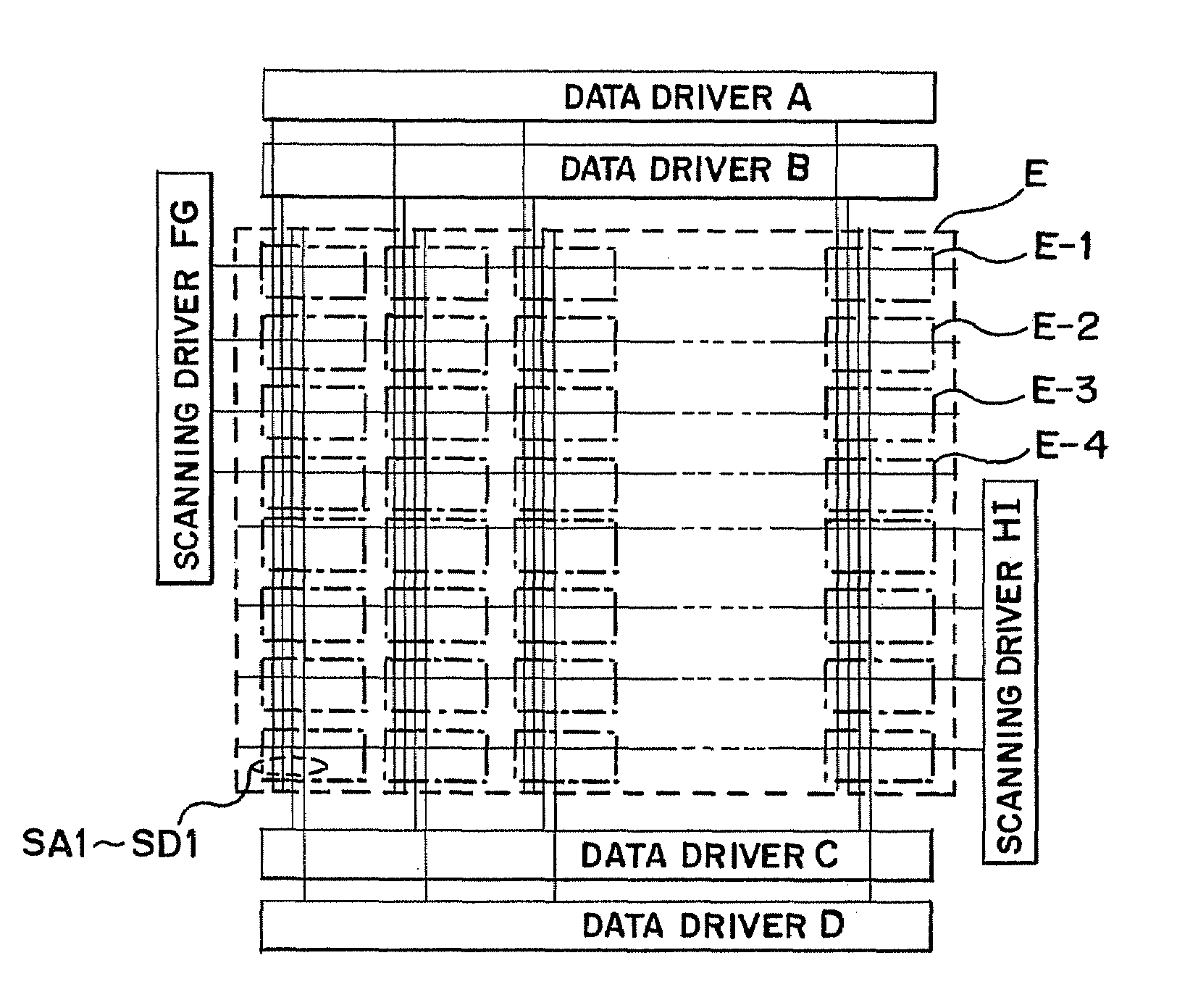
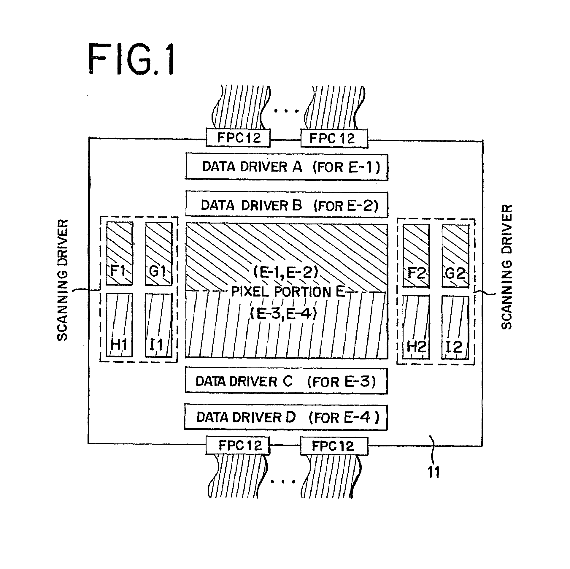
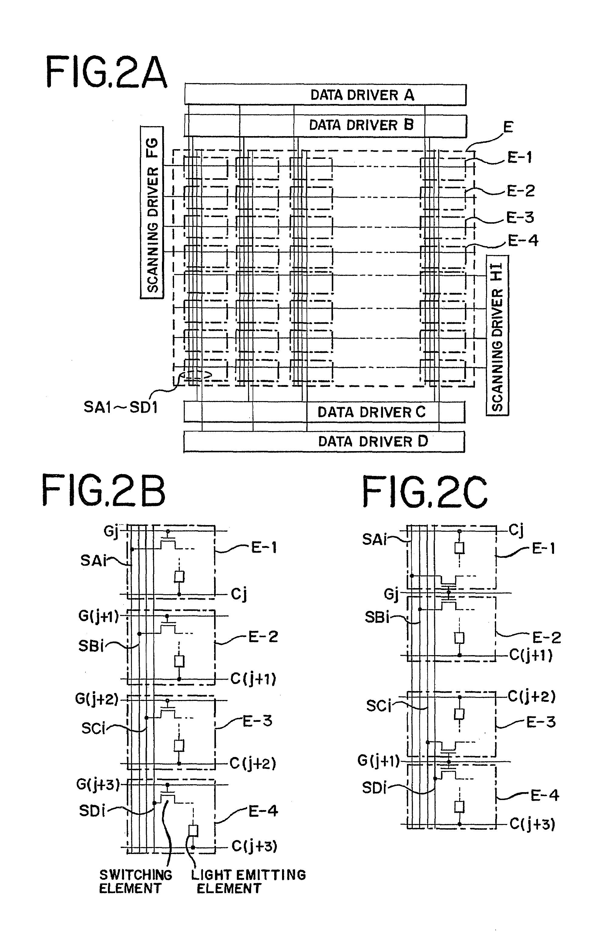
[0035]The description given first with reference to FIG. 1 is about a structural example of a display device of the present invention. The display device has a pixel portion E, which is formed on a substrate 11. The display device also has data drivers (here, four data drivers A to D) and scanning drivers (eight scanning drivers F1 to I1, F2 to I2) placed in the periphery of the pixel portion E. A pixel E-1 in the upper half of the screen is driven by the drivers A, F1, and F2 whereas a pixel E-2 in the upper half of the screen is driven by the drivers B, G1, and G2. Similarly, a pixel E-3 in the lower half of the screen is driven by C, H1, and H2 whereas a pixel E-4 in the lower half is driven by D, I1, and I2.

[0036]This mode is premised on horizontally-split driving but it is not a requisite in carrying out the present invention. However, combined ...

embodiment mode 2

[0065]Referring to FIGS. 4A and 4B and FIGS. 10A to 10D, this embodiment mode gives typical structural examples of the structure of the pixel on the i-th column and the j-th row in a pixel portion E. FIG. 10A is a general expression of a pixel circuit. Specific pixel circuit diagrams can be found in FIGS. 4A and 4B if a video signal of voltage value type is used and in FIGS. 10B to 10D if a video signal of current value type is employed.

[0066]In FIGS. 4A and 4B, a switching transistor 306 has a gate electrode connected to a scanning line Gj, a first source drain electrode connected to a signal line Si, and a second source drain electrode connected to a gate electrode of a driving transistor 307. The driving transistor 307 has a first source drain electrode connected to a power supply line Vi and a second source drain electrode connected to one of electrodes of a light emitting element 308. The other electrode of the light emitting element 308 is connected to a power supply line Cj.

[...

embodiment mode 3

[0090]This embodiment mode gives a description on a top view in FIG. 5 which shows a pixel layout for when the circuit of FIG. 4A is used in the mode illustrated in FIGS. 2A to 2C.

[0091]In FIG. 5, there are four pixels, E-1 to E-4, and data lines SAi to SDi are arranged in a column direction whereas scanning lines Gj to G(j+3) are arranged in a row direction. Each pixel has a switching TFT, a driving TFT, and a capacitor. A light emitting element connected to the driving TFT is a laminate of a pixel electrode, a light emitting layer, and an opposite electrode. Of the components of the light emitting element, the pixel electrode alone is shown in FIG. 5.

[0092]The switching TFT serves as a double gate transistor. However, the present invention is not limited thereto and the switching TFT may be a single gate transistor or a multi-gate transistor having three or more gate electrodes. In the drawing, the capacitor as a measure to hold the gate-source voltage of the driving TFT is formed...


PUM


Abstract

To provide a display device and its driving method free from lack of writing time, which usually accompanies an increase in size of a display device and enhancement in definition. Therefore, there is provided a display device and a driving method in which x (x is a natural number equal to or larger than 4) data lines are placed in each column to simultaneously supply video signals to x pixels through the x data lines. The present invention makes it possible to supply video signals to x pixels simultaneously as opposed to conventional dot sequential driving where a signal is supplied to one pixel at a time. Furthermore, a display device of the present invention and its driving method make it possible to supply video signals to (x×n) pixels at once as opposed to conventional linear sequential driving where only n pixels in the first to last (the last column is the n-th column) columns receive signals simultaneously. Thus the present invention can make the speed of writing video signals in pixels x times faster than prior art.

Description

BACKGROUND OF THE INVENTION [0001]1. Field of the Invention[0002]The present invention relates to a display device using a light emitting element and belongs to a technical field of a large-sized display device having high resolution.[0003]2. Description of the Related Art[0004]Recently, a display device for displaying an image has been more and more important. At present, a liquid crystal display device that displays an image using a liquid crystal element is widely used, taking advantages of high-definition, thinness and lightness in weight. Further, a display device (a light emitting device) using a light emitting element such as organic light emitting diode (OLED) has being developed as another display device. The light emitting device using OLED (OLED display device) draws keen attention because the light emitting device has advantages such as a high response speed, superior moving image display and a wide viewing characteristic in addition to the advantages of existing liquid ...

Claims


Application Information

Patent Timeline
Patent Type & Authority Patents(United States)
IPC IPC(8): G09G3/30G09F9/30G09G3/20H05B44/00G09G3/32H01L51/50
CPCG09G3/3233G09G3/3241G09G3/3275G09G3/2022G09G2330/02G09G2300/0426G09G2300/0809G09G2310/04G09G2300/0408
Inventor INUKAI, KAZUTAKA
Owner SEMICON ENERGY LAB CO LTD
Why Eureka
Try Eureka