Register file and its storage device

a register file and storage device technology, applied in the field of register files, can solve the problems of reducing the efficiency of demonstration tests, reducing the performance, and the inability to form scan circuits therein, and achieve the effect of reducing the scan operation tim

Inactive Publication Date: 2008-09-30
FUJITSU LTD
View PDF8 Cites 3 Cited by
  • Summary
  • Abstract
  • Description
  • Claims
  • Application Information

AI Technical Summary

Benefits of technology

[0025]In the register file according to the present invention, a memory is constituted of first storage devices which are obtained by adding shift transfer gate and output to a master flip-flop only latch in a conventional register file using master flip-flop only latch storage devices, and a scan connection configuration circuit and scan control circuit using master flip-flop only second storage devices are added thereto to realize the scan function of internally constituting a shift register and reading contents thereof in testing, thereby obtaining a merit as size reduction of the register file using master flip-flop only latch storage devices and a merit as high test / diagnosis efficiency by the internal scan function in master-slave type flip-flop (2 latches) storage devices.
[0029]Here, the decoder circuit in the scan control circuit is a write address decoder circuit in the file writing unit, and is further provided with a selector circuit for switching an input of a write address for the write address decoder circuit into an output of the counter in response to a memory array shift signal from the control unit. In this manner, the address decoder circuit in the file writing unit is used as an address decoder circuit for scan control, thereby further reducing a circuit portion to be added according to the present invention.
[0030]In the register file according to the present invention, when an address is deepened, the memory array is divided into at least two in an address direction, a shift register output terminal at the last register in the divided memory array at the front stage is connected to a shift register input terminal at the head register in the divided memory array at the rear stage, and the each divided memory array is operated in parallel by the scan control circuit. Thus, even when the number of registers in the memory array increases and the address is deepened, the memory array is divided to perform scan operation in parallel, thereby obtaining the scan processing time half the case where the memory array is not divided. Naturally, the number of divisions of the memory array can be increased to 3 or 4 as needed, thereby reducing the scan operation time depending on the number of divisions.

Problems solved by technology

In other words, when a master flip-flop only latch is assumed as a storage device, there is a merit that it can made small in size but there is a demerit that a scan circuit cannot be formed therein.
However, since the scan circuit cannot be formed therein, it is necessary to additionally design a dedicate circuit outside the register file in place of the scan circuit for chip diagnosis or demonstration test.
Thus, a gate is added to a critical path at the normal operation, causing reduction in performance.
Further, since it causes increase in chip diagnosis pattern and diagnosis time for defective inspection, causing reduction in efficiency for demonstration test, increase in manufacture cost is finally caused.
This causes reduction in performance and increase in cost.
The fact that options of the storage device structure for the register file are extremes is a significant problem in designing a semiconductor chip.
If the determination is erroneous and some change is required in the middle of the design, a large change in mounting is caused and terrible delay may occur.
As described above, the fact that the options of the storage device structure for the register file are extremes is a significant problem.

Method used


Image

  • Register file and its storage device
  • Register file and its storage device
  • Register file and its storage device

Examples


Embodiment Construction

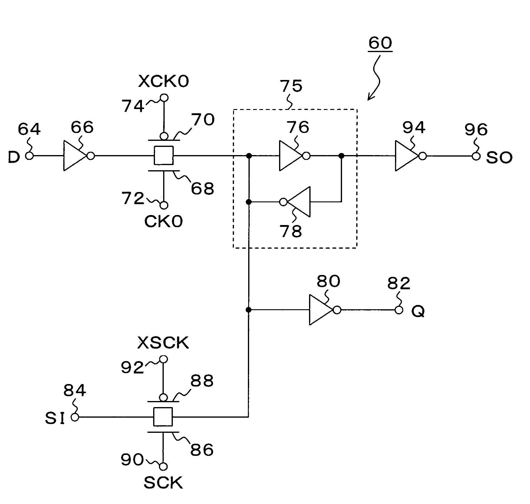
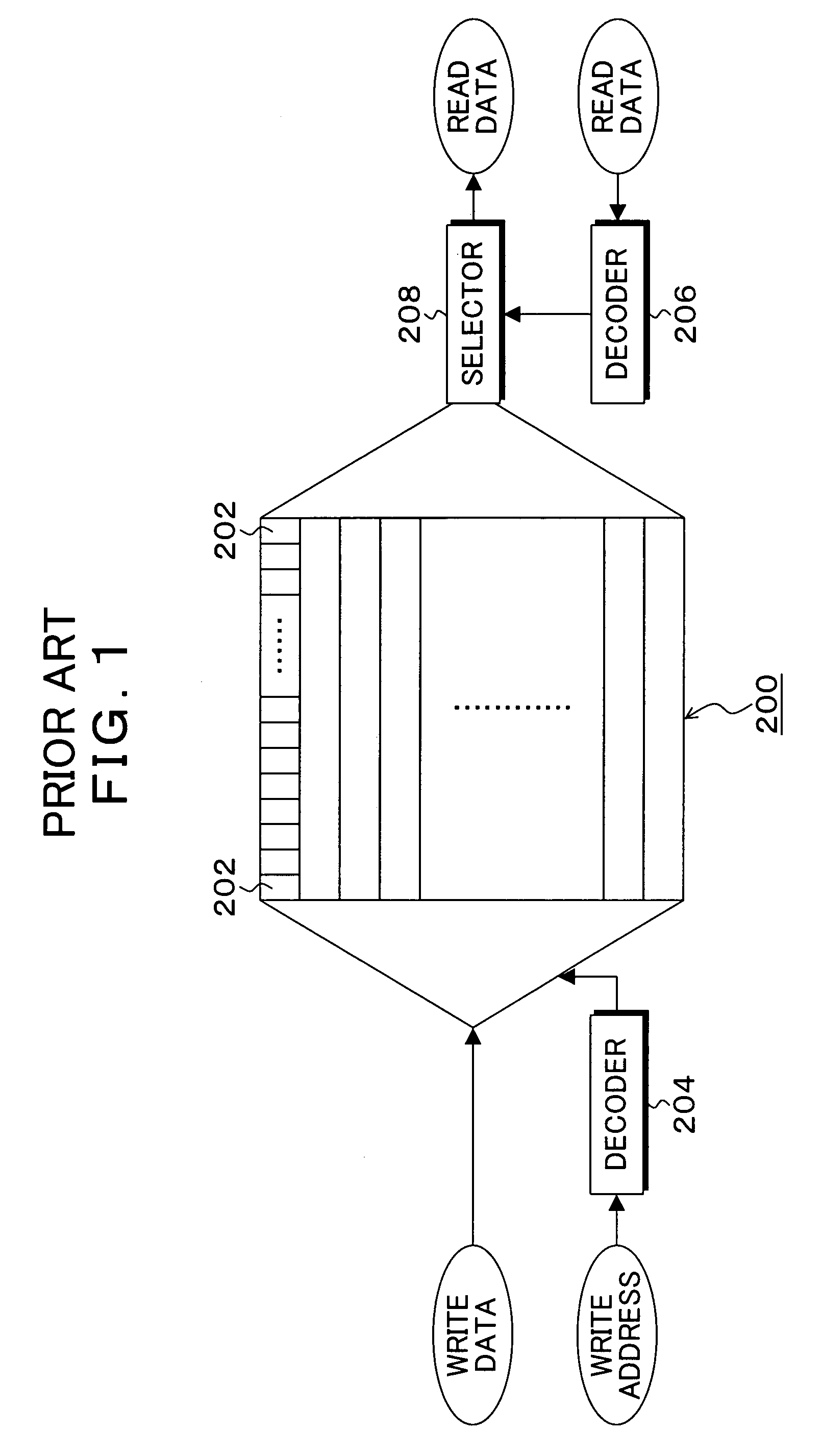
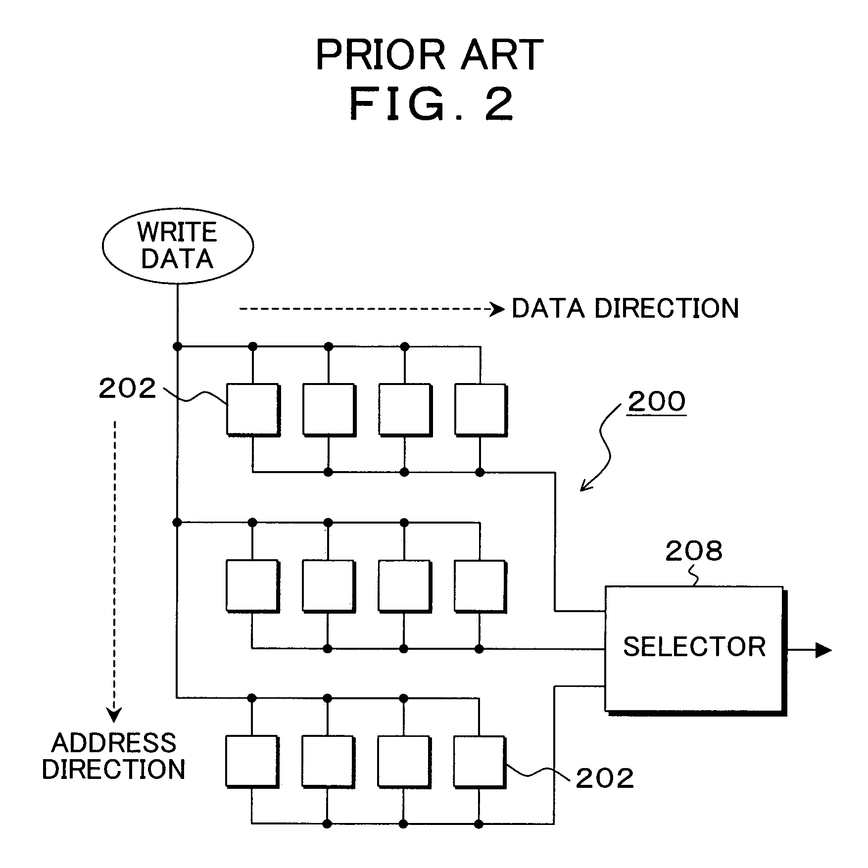
[0050]FIGS. 8A and 8B are circuit block diagrams of an embodiment of a register file according to the present invention. In FIGS. 8A and 8B, the register file according to the present invention has a memory array 10, and the memory array 10 is provided with registers 12-0, 12-1, 12-2, . . . , 12-m with the vertical direction as the address direction and the horizontal direction as the data direction. The registers 12-0 to 12-m arrange n+1 storage devices (first storage devices) in the data direction as the horizontal direction. A write address decoder circuit 24 and AND gates 26-0 to 26-m are provided as file writing units at the left of the memory array 10. A write address of the register is input into the write address decoder circuit 24 via a scan control circuit 16 according to the present invention described below from an address terminal 34, and this write address is decoded to generate a decode output for any one of the registers 12-0 to 12-m. Each decode output from the writ...


PUM


Abstract

A register file device has a memory array, a scan connection configuration circuit, a file writing unit, a file reading unit, and a scan control circuit. The memory includes first storage devices which are obtained by adding shift transfer gate and an output gate to a master flip-flop only latch in a conventional register file using master flip-flop only latch storage devices, and a scan connection configuration circuit and a scan control circuit using master flip-flop only second storage devices are added thereto to realize the scan function of internally constituting a shift register and reading contents thereof in testing. The size of the register file is reduced by using master flip-flop only latch storage devices, and a high test / diagnosis efficiency is achieved by using the internal scan function in master-slave type flip-flop (2 latches) storage devices.

Description

[0001]This application is a continuation of PCT / JP03 / 11410, filed Sep. 8, 2003.TECHNICAL FIELD[0002]The present invention relates to a register file and its storage device used as a register in a CPU, MPU or the like, and particularly to a register file integrally comprising a scan circuit for serially connecting storage devices on testing to constitute a shift register, and reading contents thereof, and its storage device.BACKGROUND ART[0003]Conventionally, there has been employed a register file which is a storage apparatus which is a collection of storage devices and in which reading can be performed faster than in DRAM or SRAM as a register of a computer such as CPU or MPU. A circuit for this register file is designed to be small and to operate at high speed, and is configured so that diagnosis on manufacturing a semiconductor chip is performed at high speed and high efficiency, thereby achieving improvement in performance of the semiconductor chip and reduction in manufacturing...

Claims


Application Information

Patent Timeline
Patent Type & Authority Patents(United States)
IPC IPC(8): G11C29/00G11C7/00G01R31/28G01R31/3185G06F11/22G06F12/16G11C29/48
CPCG01R31/318536G01R31/318544G11C29/48G01R31/318552G11C2029/3202
Inventor TANAKA, TOMOHIRO
Owner FUJITSU LTD
Why Eureka
Try Eureka