Transparent microporous materials for CMP

a micro-porous material and micro-porous material technology, applied in the direction of grinding machine components, manufacturing tools, lapping machines, etc., can solve the problems of unsatisfactory polishing defects, stable decrease of optical transmittance during the lifetime of the polishing pad,

Inactive Publication Date: 2008-10-14
CMC MATERIALS INC
View PDF52 Cites 32 Cited by
  • Summary
  • Abstract
  • Description
  • Claims
  • Application Information

AI Technical Summary

Problems solved by technology

Polishing pad windows made of a solid polyurethane are easily scratched during chemical-mechanical polishing, resulting in a steady decrease of the optical transmittance during the lifetime of the polishing pad.
This is particularly disadvantageous because the settings on the endpoint detection system must be constantly adjusted to compensate for the loss in optical transmittance.
In addition, pad windows, such as solid polyurethane windows, typically have a slower wear rate than the remainder of the polishing pad, resulting in the formation of a “lump” in the polishing pad which leads to undesirable polishing defects.

Method used


Image

  • Transparent microporous materials for CMP

Examples


Embodiment Construction

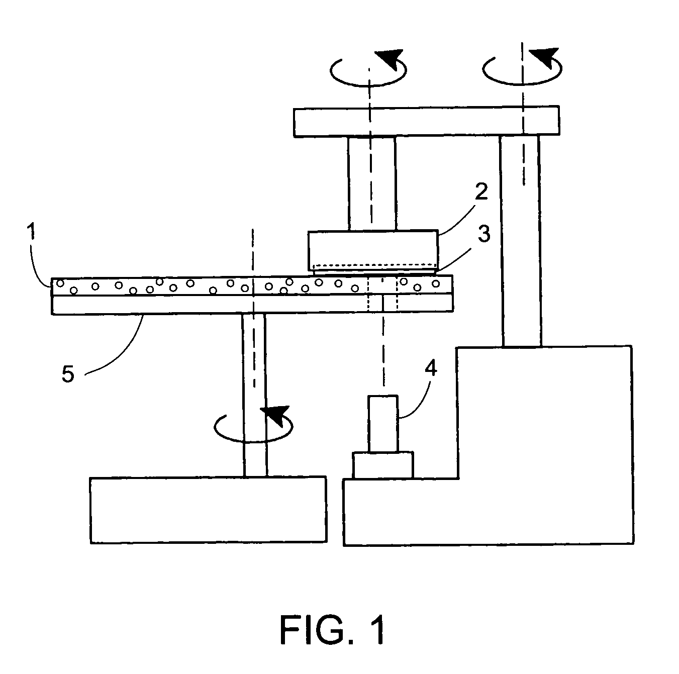
[0009]The invention is directed to a chemical-mechanical polishing pad substrate comprising a porous material, wherein the polishing pad substrate has at least a certain degree of transparency. The polishing pad substrate can be a portion within a polishing pad, or the polishing pad substrate can be an entire polishing pad (e.g., the entire polishing pad or polishing top pad is transparent). In some embodiments, the polishing pad substrate consists of, or consists essentially of, the porous material. The polishing pad substrate comprises a volume of the polishing pad that is at least 0.5 cm3 (e.g., at least about 1 cm3).

[0010]The porous material of the polishing pad substrate has an average pore size of about 0.01 microns to about 1 micron. Preferably, the average pore size is about 0.05 microns to about 0.9 microns (e.g., about 0.1 microns to about 0.8 microns). While not wishing to be bound to any particular theory, it is believed that pore sizes greater than about 1 micron will s...


PUM

PropertyMeasurementUnit
pore sizeaaaaaaaaaa
light transmittanceaaaaaaaaaa
pore sizeaaaaaaaaaa

Abstract

The invention is directed to a chemical-mechanical polishing pad substrate comprising a porous material having an average pore size of about 0.01 microns to about 1 micron. The polishing pad substrate has a light transmittance of about 10% or more at at least one wavelength of about 200 nm to about 35,000 nm. The invention is further directed to a polishing pad comprising the polishing pad substrate, a method of polishing comprising the use of the polishing pad substrate, and a chemical-mechanical apparatus comprising the polishing pad substrate.

Description

FIELD OF THE INVENTION[0001]This invention pertains to a polishing pad substrate comprising a transparent porous material for use with in situ chemical-mechanical polishing detection methods.BACKGROUND OF THE INVENTION[0002]Chemical-mechanical polishing (“CMP”) processes are used in the manufacturing of microelectronic devices to form flat surfaces on semiconductor wafers, field emission displays, and many other microelectronic substrates. For example, the manufacture of semiconductor devices generally involves the formation of various process layers, selective removal or patterning of portions of those layers, and deposition of yet additional process layers above the surface of a semiconducting substrate to form a semiconductor wafer. The process layers can include, by way of example, insulation layers, gate oxide layers, conductive layers, and layers of metal or glass, etc. It is generally desirable in certain steps of the wafer process that the uppermost surface of the process la...

Claims


Application Information

Patent Timeline
Patent Type & Authority Patents(United States)
IPC IPC(8): B24D11/00B24B1/00B24D5/00B24B29/00B24B37/24B24B49/12B24D7/12H01L21/304
CPCB24B37/24B24B37/26B24B37/04H01L21/304
Inventor PRASAD, ABANESHWAR
Owner CMC MATERIALS INC
Why Eureka
Try Eureka