Check patentability & draft patents in minutes with Patsnap Eureka AI!

Wafer pre-alignment apparatus and method

a pre-alignment and wafer technology, applied in the field of pre-alignment apparatuses, can solve the problems of high system diameter, high system efficiency, and inability to realize the downsizing,

Inactive Publication Date: 2008-10-14
YASKAWA DENKI KK
View PDF6 Cites 4 Cited by
  • Summary
  • Abstract
  • Description
  • Claims
  • Application Information

AI Technical Summary

Benefits of technology

This configuration enables efficient and accurate wafer alignment by simplifying hardware and reducing CPU processing burden, preventing repeated measurements at the same position due to uneven rotation, thereby enhancing system effectiveness and throughput.

Problems solved by technology

Thus, it is impossible to realize the downsizing, cost reduction, effectiveness of the system, and high speed of the system.
This leads to a serious problem in order to increase the diameter of the wafer and improve the throughput thereof.

Method used


Image

  • Wafer pre-alignment apparatus and method
  • Wafer pre-alignment apparatus and method
  • Wafer pre-alignment apparatus and method

Examples


Embodiment Construction

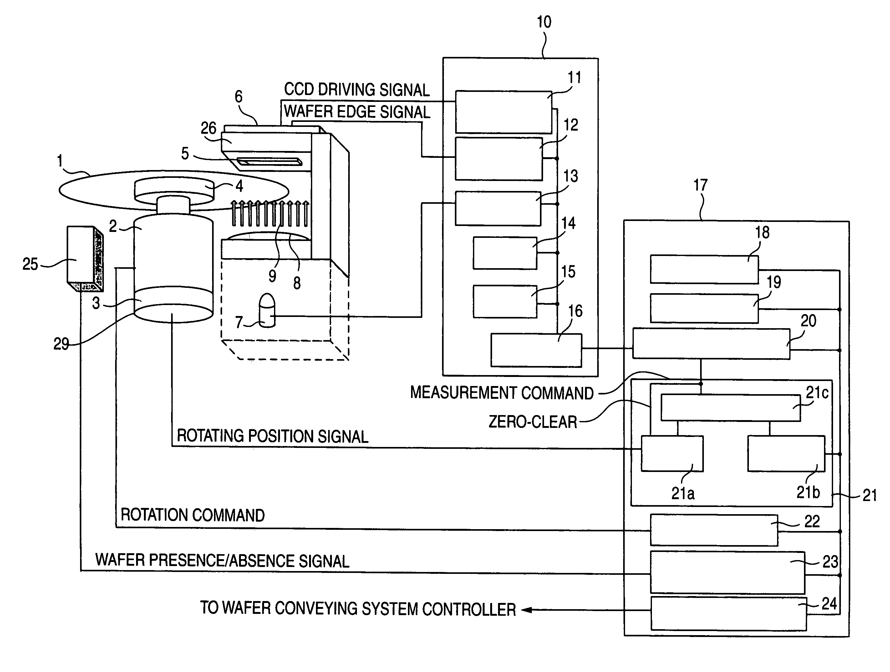
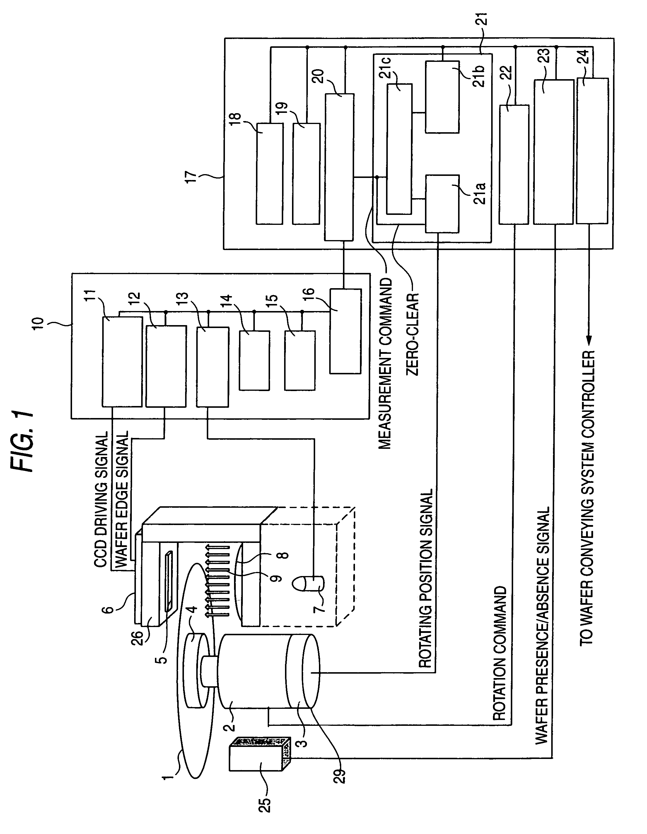
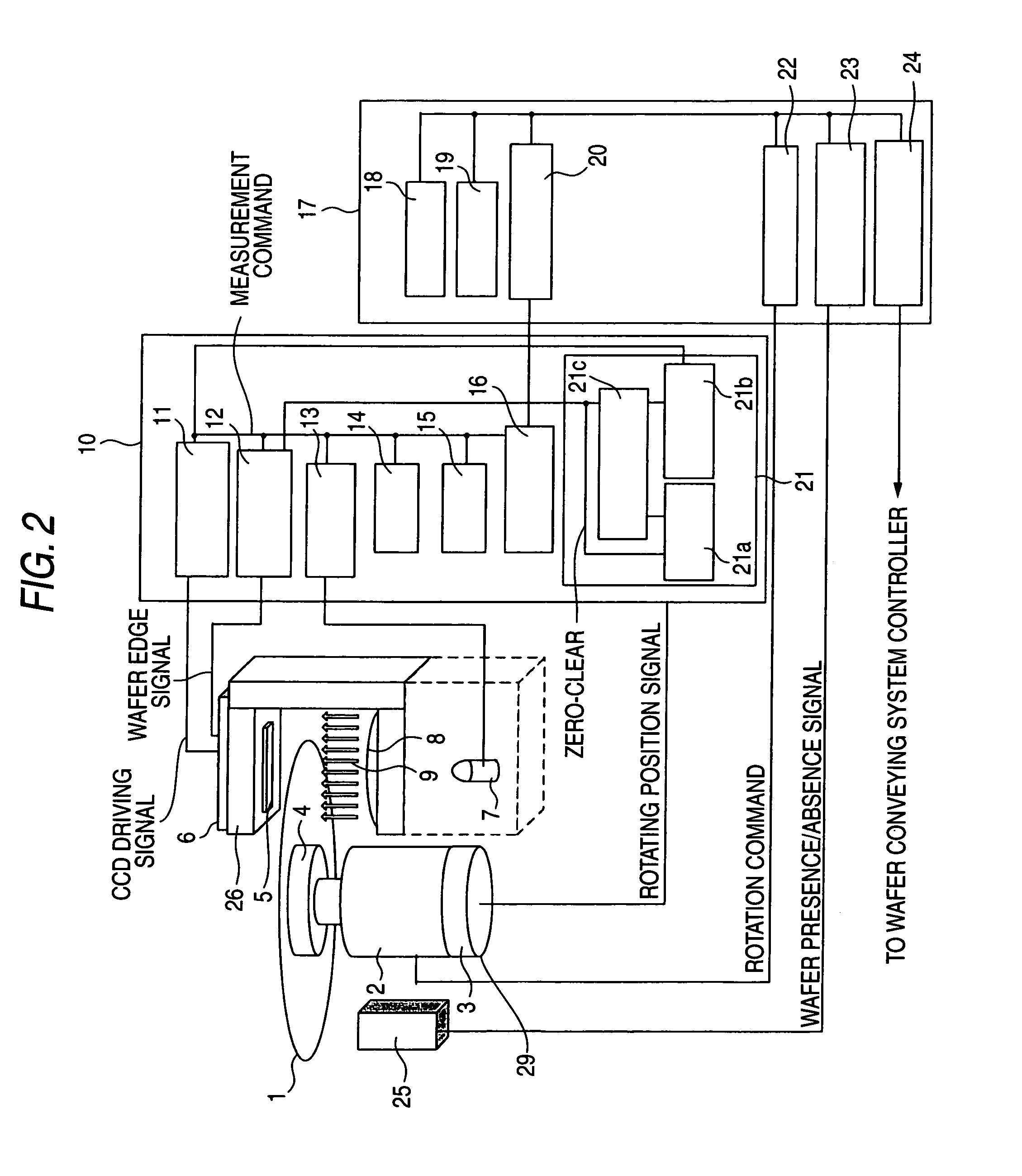
[0023]Now referring to the drawings, an explanation will be given of embodiments of this invention. FIG. 1 is a block diagram showing the configuration of a first embodiment of this invention.

[0024]FIGS. 3(a) and 3(b) are timing charts for explaining the encoder processing unit according to this invention.

[0025]In FIG. 1, a wafer positioning mechanism 29 includes a motor 2, a table 4 which is rotated by the motor 2 to hold a measured object or a wafer thereon and an encoder 3 connected to the motor to detect the rotating position of the motor 2. A pre-alignment sensor 26 includes a frame with a side of U-shape, a light source 7, a lens 8 for collimating the light emitted from the light source 7, and a CCD linear sensor 5 for receiving the light received, these components being located beneath the frame. The CCD linear sensor 5 including a large number of pixel arranged linearly in a prescribed order. The pixels of the CCD linear sensor 5 are scanned successively from the first pixel...


PUM

PropertyMeasurementUnit
diameteraaaaaaaaaa
angleaaaaaaaaaa
angle settingaaaaaaaaaa

Abstract

A wafer pre-alignment apparatus according to this invention includes a wafer rotating member, a rotation detecting member, a light emitting member for emitting light toward the periphery of the wafer, a COD linear sensor linearly arranged and signal processing member for detecting the edge position of the wafer to acquire at least one of an orientation flat position, notch position and center position of the wafer on the basis of the edge position detected, and further includes an up-down counter for converting a signal received from the rotation detecting member into rotating position information, a measured angle setting register for storing the rotation position information when the wafer rotating member rotates by an interval angle and a comparator for comparing a set value in the measured angle setting register and a counted value in the up-down counter.

Description

TECHNICAL FIELD[0001]This invention relates to a pre-alignment apparatus which is employed in a semiconductor manufacturing apparatus and serves to detect / position the position of a disk-shaped semiconductor wafer and the positions of orientation flat, notch, etc. thereof.RELATED ART[0002]Referring to FIG. 4, an explanation will be given of the configuration of a prior art pre-alignment sensor apparatus. In FIG. 4, a table 4 secured to the upper tip of the axis of a motor 2 is adapted to be movable. When a wafer 1 is placed on the table 4, it can intervene between a light source 7 which is located on the lower side of the outer peripheral region of the wafer and a CCD linear sensor 5 which is a light receiving unit located on the upper side thereof. A pre-alignment sensor 26 includes a light source 7, a lens 8, the CCD linear sensor 5, a substrate 6 on which the CCD linear sensor is mounted, and a frame with a side of U-shape which fixes these components. The light emitted from the ...

Claims


Application Information

Patent Timeline
Patent Type & Authority Patents(United States)
IPC IPC(8): G01B11/00G03F9/00H01L21/027H01L21/68H01L23/544
CPCG03F9/7011H01L21/681H01L2223/54493H01L23/544H01L2924/0002H01L2924/00H01L21/68
Inventor INENAGA, MASAMICHIKATSUDA, SHINICHIARINAGA, YUJI
Owner YASKAWA DENKI KK
Features
  • R&D
  • Intellectual Property
  • Life Sciences
  • Materials
  • Tech Scout
  • Unparalleled Data Quality
  • Higher Quality Content
  • 60% Fewer Hallucinations
Learn More